
| Parameter | Specification |
|---|---|
| Industrial LPDDR4X SDRAM | Ultra-low-power memory at 0.6 V I/O delivering up to 4266 MT/s in a compact dual-channel package, ideal for bandwidth-intensive yet power-sensitive designs. |
- JEDEC Compliant
- Industrial & Extended Temp
- −40°C to 85°C & −55°C to 105°C
- 2-8GB
Ningbo Loongtion Intelligent Technology Co., Ltd.
hi@loongtion.com | www.loongtion.com
Document Version 3.2 | June 2026
1. Executive Summary
The Loongtion LPDDR4X SDRAM is a low-power, high-bandwidth memory solution designed for industrial, embedded, military-grade, and commercial systems requiring robust performance across extended temperature ranges. Based on traditional DDR SDRAM technology with architectural improvements in power efficiency and data throughput, this product utilizes wafer sourced from ChangXin Memory Technologies and is packaged to meet China-domestic supply compliance requirements.
Key differentiators include a dual-channel architecture per die, a Low Voltage Swing Terminated Logic (LVSTL) I/O system, and support for multiple temperature grades ranging from standard (-40°C to 85°C) and extended (85°C to 105°C) to industrial/military (-55°C to 105°C). The device operates at core voltages of VDD1 = 1.8 V, VDD2 = 1.1 V, and I/O voltage VDDQ = 0.6 V, enabling significant power savings while supporting data rates up to 4266 MT/s across all listed part numbers.
Loongtion LPDDR4X SDRAM is suitable for applications requiring low power, high bandwidth, and supply-chain localization. All part numbers are offered in a compact FBGA200 package measuring 15 mm × 10 mm × 0.95 mm.
2. Product Overview
Loongtion LPDDR4X SDRAM (Low Power Double Data Rate 4X Synchronous Dynamic Random Access Memory) is a high-performance memory product belonging to the LPDDR4X category. It is fabricated using advanced process technology and is delivered in an FBGA200 package with a 22-row ball grid array (ball pitch 0.8 mm along the X-axis and 0.65 mm along the Y-axis). The physical dimensions are 15 mm × 10 mm × 0.95 mm.
The device supports a multi-channel architecture: dual-channel die configurations with dedicated channels A and B, or functionally equivalent single-channel die stacking. The "_A" and "_B" signal suffixes denote respective DRAM channels; "_B" pads exist only on dual-channel SDRAM devices.
Capacity and Temperature Options
| Capacity | Part Number | Package | Data Rate (MT/s) | Temperature Range |
|---|---|---|---|---|
| 2 GB | YZDB5CCBM-EA-A | FBGA200 | 3733 / 4266 | -55°C to 105°C |
| 4 GB | YZDB6CCBM-EA-A | FBGA200 | 3733 / 4266 | -55°C to 105°C |
| 2 GB | YZDB5CCBM-EA-A | FBGA200 | 3733 / 4266 | -40°C to 85°C |
| 4 GB | YZDB6CCBM-EA-A | FBGA200 | 3733 / 4266 | -40°C to 85°C |
| 4 GB | YZDB6CCBM-EA-A | FBGA200 | 3733 / 4266 | -40°C to 85°C |
| 8 GB | YZDB7CCDM-EA-A | FBGA200 | 3733 / 4266 | -40°C to 85°C |
Document Revision History
| Revision | Date | Description |
|---|---|---|
| Rev 1.0 | 2024/7/16 | Preliminary |
| Rev 2.0 | 2025/04/25 | Added 8GB LPDDR4X product |
| Rev 3.0 | 2025/12/11 | Added industrial/military-grade 2GB and 4GB product models |
| Rev 3.2 | 2026/03/02 | Added 16-bit width |
3. Technology and Architecture
Core Technology and Channel Architecture
The LPDDR4X SDRAM is based on traditional DDR SDRAM technology with enhancements specifically targeting reduced power consumption and improved data throughput. Internal design is organized as a multi-channel architecture; for example, the 4 GB configuration comprises a dual-die, dual-channel, single-rank arrangement.
Each channel provides independent command/address and data buses. Differential clock inputs (CK_t_A/CK_c_A for channel A, CK_t_B/CK_c_B for channel B) and clock enable signals (CKE_A, CKE_B) control channel activation. The command/address inputs (CA[5:0]) are shared within each channel and operate in single data rate mode.
I/O System: LVSTL
The I/O system employs Low Voltage Swing Terminated Logic (LVSTL), which consists of a pull-up driver, a pull-down driver, and an on-die terminator. Calibration is performed in two steps:
- Pull-down calibration: The NMOS pull-down device is calibrated to 240 Ω by connecting the ZQ pin through a 240 Ω ±1% resistor to VDDQ. The drive strength is increased until the ZQ pin voltage is less than VDDQ/2.
- Pull-up calibration: The NMOS pull-up device is calibrated to a VOH target value set via Mode Register Set (MRS). The ODT of the NMOS controller is configured, and drive strength increased until the data bit exceeds the VOH target.
Data Strobe and Data Mask Inversion
Each data byte has one pair of differential data strobe signals (DQS_t, DQS_c). During reads, the DRAM generates the strobe edge-aligned with data; during writes, the memory controller generates the strobe preceding data. The Data Mask Inversion (DMI) signal is bidirectional: it is driven high when data is inverted and low when normal. Data inversion can be disabled via the Mode Register. The DMI signal is also used for write data masking.
On-Die Termination (ODT)
For LPDDR4X devices, the ODT_CA pin is ignored. All ODT functions for CS, CA, and CK signals are fully controlled by Mode Registers MR11 and MR22. The ODT_CA pin should be connected to VDD2 or VSS.
Self-Refresh and Temperature Sensing
The device supports self-refresh with a 1× refresh rate before entering the high temperature range. An internal temperature sensor can be used to set the appropriate refresh rate and to determine whether AC timing derating is required.
Training and Calibration Features
Loongtion LPDDR4X SDRAM includes a comprehensive set of training and calibration functions:
- Bus Command Training (CBT) – adjusts timing for command/address signals.
- Write Leveling – aligns DQS with clock for write operations.
- Read Postamble Training – optimizes read postamble timing.
- DQS Internal Oscillator – provides timing reference for DQS.
- ZQ Calibration – calibrates output drive strength and ODT.
- Frequency Set Point (FSP) – supports multiple operating frequencies.
Mode Register Operations
Mode register read and write operations are supported with the following minimum timing:
- tMRR (Mode Register Read Cycle): 8 nCK
- tMRW (Mode Register Write Cycle): MAX(10 ns, 10 nCK)
- tMRD (Mode Register Set Command Delay): MAX(14 ns, 10 nCK)
4. Key Features and Differentiators
- Low Operating Voltages: VDD1 = 1.8 V (1.70–1.95 V), VDD2 = 1.1 V (1.06–1.17 V), VDDQ = 0.6 V (0.57–0.65 V). The sub-1 V I/O supply contributes to reduced dynamic power consumption.
- Dynamic Power Management and Deep Sleep Mode: Enables further reduction in active and standby power.
- Data Bus Inversion (DBI): Supported with both DBI Off and DBI On modes; patterns for IDD4R and IDD4W are documented.
- Multiple Temperature Grades: Standard (-40°C to 85°C), Extended (85°C to 105°C), and Industrial/Military (-55°C to 105°C) available per part number.
- China-Domestic Compliance: Package design meets domestic supply requirements; corresponding China-domestic certification documents are available.
- High Data Rate Support: All listed part numbers support operation at 3733 MT/s and 4266 MT/s.
- VREF Training: Supports VREFCA and VrefDQ internal setting values obtained through training; Vref is set by the system for Ron and ODT settings.
- 1.1V High-Speed LVCMOS (HS_LVCMOS): Supported for compatibility with common controller interfaces.
5. Technical Specifications
5.1 Package Dimensions (FBGA200)
| Parameter | Symbol | Min (mm) | Nom (mm) | Max (mm) |
|---|---|---|---|---|
| Package height | A1 | 0.85 | 0.95 | 1.05 |
| Standoff | A2 | 0.17 | 0.22 | 0.27 |
| Package length | D | 9.9 | 10.0 | 10.1 |
| Die length | D1 | — | 8.8 | — |
| Package width | E | 14.90 | 15.00 | 15.10 |
| Die width | E1 | — | 13.65 | — |
| Ball pad width | d | — | 0.80 | — |
| Ball pitch (X-axis) | — | — | 0.80 | — |
| Ball pitch (Y-axis) | e | — | 0.65 | — |
| Ball diameter | b | 0.26 | 0.31 | 0.36 |
5.2 Operating Voltage Ranges
| Supply | Parameter | Min (V) | Typ (V) | Max (V) |
|---|---|---|---|---|
| VDD1 | Core Voltage 1 | 1.70 | 1.80 | 1.95 |
| VDD2 | Core Voltage 2 | 1.06 | 1.10 | 1.17 |
| VDDQ | I/O Supply Voltage | 0.57 | 0.60 | 0.65 |
Note: VDD2 range of 1.06 V to 1.17 V applies to datasheet sections 9.3 and 9.4; VDDQ range of 0.57 V to 0.65 V applies to sections 9.5 and 9.6.
5.3 Absolute Maximum Ratings
| Parameter | Min (V) | Max (V) |
|---|---|---|
| VDD1 Supply Voltage | -0.4 | 2.1 |
| VDD2 Supply Voltage | -0.4 | 1.5 |
| VDDQ Supply Voltage | -0.4 | 1.5 |
| Other pins (VIN, VOUT) | -0.4 | 1.5 |
Warning: Stresses beyond absolute maximum ratings may cause permanent damage. Operation at maximum rating conditions for extended periods may affect device reliability.
5.4 Leakage Current
| Parameter | Min | Max |
|---|---|---|
| Input Leakage Current (IL) | -4 µA | 4 µA |
| Input/Output Leakage Current (IOZ) | -5 µA | 5 µA |
5.5 IDD Current Specifications (at 4266 Mbps, Dual-Channel, Single Die)
| Parameter | VDD1 (mA) | VDD2 (mA) | VDDQ (mA) |
|---|---|---|---|
| IDD01 | 2.6 | — | — |
| IDD02 | — | 41.5 | — |
| IDD0Q | — | — | 1.2 |
| IDD4R2 (burst read) | — | 284.2 | — |
| IDD4RQ (burst read) | — | — | 91.9 |
| IDD4W2 (burst write) | — | 235.2 | — |
| IDD52 (all bank refresh burst) | — | 105.4 | — |
| IDD6 @25°C (self-refresh) | 0.6 | 3.3 | 0.1 |
| IDD6 @85°C (self-refresh) | 0.8 | 5.2 | 0.1 |
- IDD6 at 85°C is guaranteed; IDD6 at 45°C is typical (arithmetic mean distribution).
- IDD6ET (85°C to 105°C) is typical, sample value only, not tested.
- IDD parameters apply over full operating voltage and temperature ranges (except IDD6ET).
- Dual-channel devices are specified for dual-channel operation with both channels running simultaneously.
- Output load = 5 pF, RON = 40 Ω for IDD4R; ODT disabled: MR11[2:0]=000B.
5.6 Supported Data Rates
| Data Rate (MT/s) | Notes |
|---|---|
| 1600 | Referenced in timing tables |
| 1866 | Referenced in timing tables |
| 2133 | Referenced in timing tables |
| 2400 | Referenced in timing tables |
| 2667 | Referenced in timing tables |
| 3200 | Referenced in timing tables |
| 3733 | Supported for all listed part numbers |
| 4266 | Supported for all listed part numbers |
5.7 Clock Timing (at 4266 Mbps)
| Parameter | Symbol | Min | Max |
|---|---|---|---|
| Average clock period | tCK(avg) | 0.468 ns | 100 ns |
Note: Variation of tCK(avg) over 200 clock cycles can be up to ±1 %, provided all jitter and timing specifications are met. Average high pulse width (tCH(avg)) and average low pulse width (tCL(avg)) are defined in the datasheet; numerical min/max values are not specified in the source documentation.
5.8 Core Timing Parameters
| Parameter | Symbol | Min | Max |
|---|---|---|---|
| CAS-to-CAS delay | tCCD | 8 tCK(avg) | — |
| RAS to CAS Delay | tRCD | (18 ns, 4 nCK) | — |
| Row Precharge Time (Single Bank) | tRPpb | (18 ns, 4 nCK) | — |
| Row Precharge Time (All Banks) | tRPab | (21 ns, 4 nCK) | — |
| Row Active Time | tRAS | (42 ns, 3 nCK) | (9×tREFI, 70.2 µs) |
| Write Recovery Time | tWR | (18 ns, 6 nCK) | — |
| Write-to-Read Delay | tWTR | (10 ns, 8 nCK) | — |
| Activate Bank A to Activate Bank B | tRRD | (10 ns, 4 nCK) | — |
| Precharge to Precharge Delay | tPPD | 4 tCK | — |
| Four-Bank Activation Window | tFAW | 40 ns | — |
5.9 Read and Write Timing Parameters (Selected)
| Parameter | Symbol | Min | Max |
|---|---|---|---|
| DQS output access time from CK_t/CK_c | tDQSCK | 1.5 ns | 3.5 ns |
| DQS-DQ skew | tDQSQ | — | 0.18 UI |
| Write command to first DQS latching edge | tDQSS | 0.75 tCK(avg) | 1.25 tCK(avg) |
| Read preamble time | tRPRE | 1.8 tCK(avg) | — |
| Read postamble time (0.5 tCK) | tRPST | 0.4 tCK(avg) | — |
| Write postamble time | tWPRE | 1.8 tCK(avg) | — |
5.10 Temperature Ranges
| Grade | Temperature Range | Applicable Part Numbers |
|---|---|---|
| Standard | -40°C to 85°C | YZDB5CCBM-EA-A, YZDB6CCBM-EA-A, YZDB6CCBM-EA-A, YZDB7CCDM-EA-A |
| Extended | 85°C to 105°C | All standard-grade parts (derating applies) |
| Industrial/Military | -55°C to 105°C | YZDB5CCBM-EA-A, YZDB6CCBM-EA-A |
Note: Operating temperature is defined as the case surface temperature at the center top of the LPDDR4X device.
5.11 Input/Output Capacitance (die only, at 3200–4266 MT/s)
| Pin | Symbol | Min (pF) | Max (pF) |
|---|---|---|---|
| CK_t and CK_c | CCK | 0.5 | 0.9 |
| All other input-only pins | CI | 0.5 | 0.9 |
| DQ, DMI, DQS_t, DQS_c | CIO | 0.7 | 1.3 |
| ZQ pin | CZQ | 0 | 5 |
Note: Capacitance values at 4266–3733 MT/s are not specified in source documentation (TBD).
5.12 Output Slew Rates
| Parameter | Symbol | Min | Max |
|---|---|---|---|
| Single-ended output slew rate | SRQse | 3 V/ns | 9 V/ns |
| Output slew rate matching ratio | — | 0.8 | 1.2 |
| Differential output slew rate | SRQdiff | 7 V/ns | 18 V/ns |
5.13 Input Voltage Levels (referenced to VDD2)
| Parameter | Symbol | Min | Max |
|---|---|---|---|
| AC Input High Voltage | VIH(AC) | 0.75×VDD2 | VDD2+0.2 V |
| AC Input Low Voltage | VIL(AC) | -0.2 V | 0.25×VDD2 |
| DC Input High Voltage | VIH(DC) | 0.65×VDD2 | VDD2+0.2 V |
| DC Input Low Voltage | VIL(DC) | -0.2 V | 0.2×VDD2 |
5.14 Overshoot/Undershoot Specifications
| Parameter | Value |
|---|---|
| Maximum allowed peak amplitude in overshoot region | 0.35 V |
| Maximum peak voltage allowed in undershoot region | 0.35 V |
| Maximum overshoot region above VDD/VDDQ | 0.8 V-ns |
6. Performance and Reliability
Data Rate and Bandwidth
All listed part numbers support operation at 3733 MT/s and 4266 MT/s. The device provides a 16-bit data bus per channel (DQ[15:0]). Peak bandwidth per channel is not specified in source documentation; system designers should calculate based on the supported data rates and bus width.
Self-Refresh Current
Loongtion LPDDR4X SDRAM exhibits very low self-refresh current, particularly at room temperature:
| Temperature | VDD1 (mA) | VDD2 (mA) | VDDQ (mA) |
|---|---|---|---|
| 25°C | 0.6 | 3.3 | 0.1 |
| 85°C | 0.8 | 5.2 | 0.1 |
Temperature Derating (Extended Range 85°C to 105°C)
When operating above 85°C, the following AC timing parameters must be derated:
| Parameter | Derated Minimum |
|---|---|
| DQS output access time from CK_t/CK_c (tDQSCK) | 3600 ps |
| RAS to CAS delay (tRCD) | tRCD + 1.875 ns |
| ACTIVATE to ACTIVATE command period (tRC) | tRC + 3.75 ns |
| Row active time (tRAS) | tRAS + 1.875 ns |
| Row precharge time (tRP) | tRP + 1.875 ns |
| Active group A to active group B (tRRD) | tRRD + 1.875 ns |
Reliability Parameters
The following reliability parameters are not specified in source documentation: TBW (Terabytes Written), MTBF (Mean Time Between Failures), ECC (Error Correcting Code) support, and specific endurance ratings. Users should contact Loongtion for detailed reliability data.
Output Timing Characteristics
- tDQSCK temperature variation: 4 ps/°C
- tDQSCK voltage variation: 7 ps/mV
- CK to DQS rank-to-rank delay: ≤ 1 ns
7. Applications and Target Markets
Loongtion LPDDR4X SDRAM is suitable for industrial and military-grade applications requiring low power, high bandwidth, and robust temperature tolerance. The device is available in standard (-40°C to 85°C) and industrial/military (-55°C to 105°C) temperature grades. Industrial and military-grade product models (2GB and 4GB) are available. Additional application details are not specified in the source documentation; contact Loongtion for specific use cases.
8. System Integration and Design Considerations
Pin Connection Requirements
- ZQ pin: Must be connected to VDDQ through a 240 Ω ±1% resistor for calibration.
- ODT_CA pin: For LPDDR4X devices, this pin is ignored. It should be connected to VDD2 or VSS. ODT for CS/CA/CK is fully controlled via MR11 and MR22.
Power Supply Isolation
The three power supplies (VDD1, VDD2, VDDQ) are isolated from each other. Proper decoupling is required for each supply rail to meet the specified voltage tolerances.
Signal Integrity Requirements
- Differential clock and DQS signals must maintain monotonic slope through the input switching region.
- For differential clocks at 3733/4266 MT/s, the minimum differential input voltage is 360 mV, and the single-ended clock input voltage must be at least 180 mV.
- For DQS at 3733/4266 MT/s, the minimum differential input voltage is 340 mV.
- Overshoot and undershoot must be limited to 0.35 V peak amplitude and 0.8 V-ns overshoot region above VDD/VDDQ.
Receiver Mask Definitions
- The CA receiver mask defines the region where input signals must not intrude for correct capture. The center of the cumulative data input eye (Vcent) defines the reference level.
- The DQ receiver mask similarly defines valid input regions with total timing and voltage windows (TdiVW_total, VdIVW_total) for a target bit error rate.
- Vref is set by the system for Ron and ODT settings.
Timing Derating for High Temperature
Designs operating at case temperatures above 85°C must apply the derating values listed in Section 6. The internal temperature sensor can be used to trigger refresh rate adjustments and to enable derating logic.
Self-Refresh Usage
The device supports self-refresh entry and exit with the following AC timing:
| Parameter | Symbol | Min |
|---|---|---|
| Delay from SRE command to CKE input low | tESCKE | (1.75 ns, 3 tCK) |
| Minimum self-refresh time | tSR | (15 ns, 3 tCK) |
| Exit self-refresh to active command | tXSR | (tRFCab + 7.5 ns, 2 tCK) |
Simulation Guidance
During circuit design, IBIS or other simulation tools should be used to correlate the timing reference load with the actual system environment.
9. Standards Compliance and Quality
China-Domestic Compliance
Loongtion LPDDR4X SDRAM is designed and packaged to meet China-domestic supply requirements. Corresponding China-domestic certification documents are available upon request.
Wafer Source
Wafer production is sourced from ChangXin Memory Technologies.
Storage Temperature
The storage temperature range is -55°C to 125°C.
JEDEC Compliance
Specific JEDEC compliance status (e.g., JEDEC LPDDR4X standard) is not explicitly stated in the source documentation. The device follows conventional LPDDR4X electrical and timing parameters as described in this document.
Quality Parameters
Detailed quality parameters (ESD tolerance, RoHS compliance, reliability test data) are not specified in the source documentation. For current quality and compliance information, contact Loongtion at hi@loongtion.com.
10. Ordering Information
| Capacity | Part Number | Package | Data Rate (MT/s) | Temperature Range | Grade |
|---|---|---|---|---|---|
| 2 GB | YZDB5CCBM-EA-A | FBGA200 | 3733 / 4266 | -55°C to 105°C | Industrial/Military |
| 4 GB | YZDB6CCBM-EA-A | FBGA200 | 3733 / 4266 | -55°C to 105°C | Industrial/Military |
| 2 GB | YZDB5CCBM-EA-A | FBGA200 | 3733 / 4266 | -40°C to 85°C | Standard |
| 4 GB | YZDB6CCBM-EA-A | FBGA200 | 3733 / 4266 | -40°C to 85°C | Standard |
| 4 GB | YZDB6CCBM-EA-A | FBGA200 | 3733 / 4266 | -40°C to 85°C | Standard |
| 8 GB | YZDB7CCDM-EA-A | FBGA200 | 3733 / 4266 | -40°C to 85°C | Standard |
- All part numbers support dual-channel operation.
- Additional ordering information (marking code, packaging options, tape/reel) is not specified in the source documentation. Contact Loongtion for details.
11. About Loongtion
Ningbo Loongtion Intelligent Technology Co., Ltd. (Loongtion®) is a supplier of China-domestic memory and solid-state storage products for industrial, embedded, medical, and commercial applications. The company’s product portfolio includes:
- DDR3 / DDR4 / DDR5 / LPDDR4X SDRAM
- eMMC 5.1 embedded storage
- M.2 NVMe SSDs
- NVMe BGA SSDs
Loongtion focuses on delivering reliable, temperature-robust memory solutions that meet the growing demand for localized supply chains in the Chinese market.
Contact Information:
- Email: hi@loongtion.com
- Website: www.loongtion.com
*Disclaimer: This whitepaper is based on the consolidated technical fact sheet provided by Ningbo Loongtion Intelligent Technology Co., Ltd. Specifications are subject to change without notice. Users should refer to the latest official datasheet for current parameters and ordering information. Loongtion assumes no liability for any errors or omissions in this document.*
Related products
Shortlist lines referenced in this guide — open the product page for PN, grades, and datasheet request.
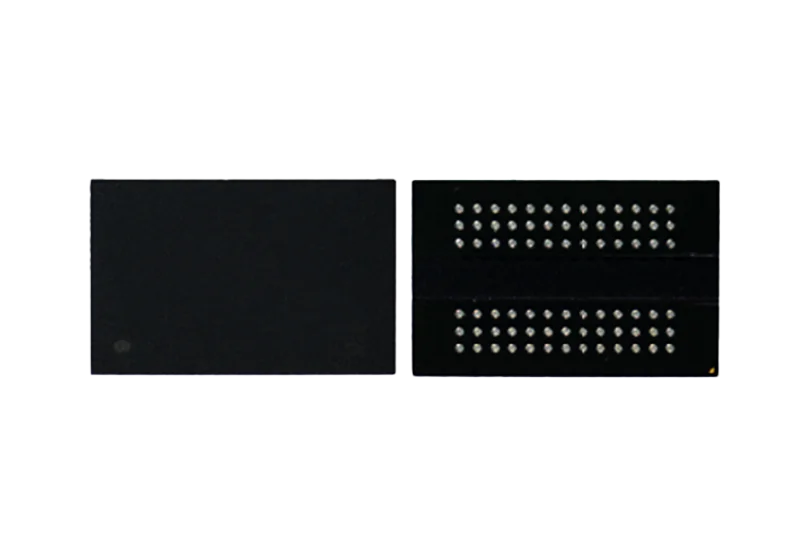
8Gb DDR4 DRAM Chip · Wide-temp
- Both wafer and package
- FBGA78/FBGA96 package
- Supports VDD(VDDQ) 1.2V +/-
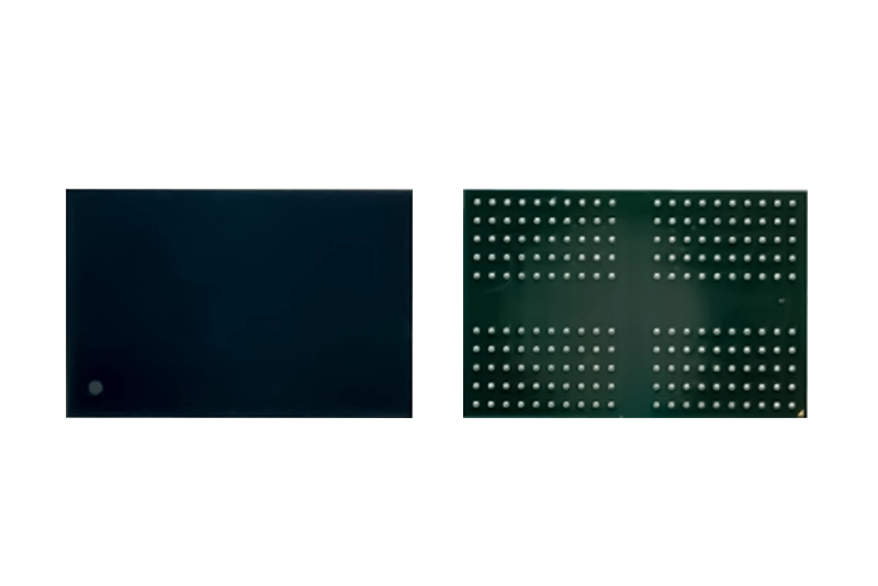
LPDDR4X DRAM Chip
- Slim FBGA178/FBGA200 package
- 0.6V core ultra-low voltage
- 100% domestic solution
Related resources
Continue with related selection guides and notes for the same industrial memory topic.
Related cross-references
Pin-to-pin and functional alternatives referenced from this guide — for BOM review, dual-sourcing, or EOL coverage.