
| Parameter | Specification |
|---|---|
| Industrial eMMC 5.1 Embedded Flash | Integrated controller-and-flash embedded storage with LDPC ECC, HS400 up to 200 MHz, and pSLC or TLC options for mission-critical reliability or high-capacity cost efficiency. |
- JEDEC Compliant
- Industrial & Extended Temp
- −40°C to 85°C & −55°C to 105°C
- 8-256GB
Ningbo Loongtion Intelligent Technology Co., Ltd.
hi@loongtion.com | www.loongtion.com
Document Version 3.0 | June 2026
2. Product Overview
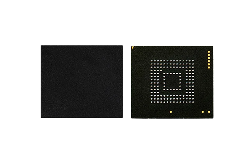
The Loongtion eMMC 5.1 is a complete embedded storage solution that combines a NAND flash controller and NAND flash die in a single ball-grid-array (BGA) package. It provides a standardized interface through a 12-line bus (CLK, CMD, Data Strobe, 8-bit data bus, and hardware reset). The device supports multiple bus widths (1-bit, 4-bit, 8-bit) and all eMMC 5.1 defined data transfer modes, including HS400 at 1.8 V with a 200 MHz clock.
2.1 Part Number Overview
| Part Number | Capacity | Flash Type | Temperature Range | Package |
|---|---|---|---|---|
| YMDL008MNS-S | 8 GB | pSLC | –55 °C to +105 °C | 153FBGA |
| YMDL016MNS-S | 16 GB | pSLC | –55 °C to +105 °C | 153FBGA |
| YMDL032MNS-S | 32 GB | pSLC | –55 °C to +105 °C | 153FBGA |
| YMDL064MNS-S | 64 GB | pSLC | –55 °C to +105 °C | 153FBGA |
| YIDL032MNT-S | 32 GB | TLC | –40 °C to +85 °C | 153FBGA |
| YIDL064MNT-S | 64 GB | TLC | –40 °C to +85 °C | 153FBGA |
| YIDL128MNT-S | 128 GB | TLC | –40 °C to +85 °C | 153FBGA |
| YIDL256MNT-S | 256 GB | TLC | –40 °C to +85 °C | 153FBGA |
2.2 CID Register Fields (Device Identification)
The Card Identification (CID) register is programmed during manufacturing. Key fields include:
| Field | Value | Notes |
|---|---|---|
| Manufacturer ID (MID) | FFh | Assigned to Loongtion |
| Card/BGA Type (CBX) | 01h | BGA package |
| OEM/User ID (OID) | FFh | Not fixed |
| Product Name (PNM) | FFFFFFh | – |
| Product Revision (PRV) | FFh | Not fixed |
| Product Serial Number (PSN) | Production random | – |
| Manufacturing Date (MDT) | Month, year | Not fixed |
| CRC7 Checksum (CRC) | 00h | Not fixed |
2.3 Document Revision History
| Revision | Date | Key Changes |
|---|---|---|
| Rev 1.0 | 2021/12/10 | Initial release |
| Rev 1.2 | 2022/09/23 | Product naming errata correction |
| Rev 1.3 | 2023/05/23 | Added 64 GB pSLC product specification |
| Rev 1.4 | 2023/10/07 | Added BGA100 package specification |
| Rev 2.0 | 2024/12/05 | Removed BGA100 package and storage temperature |
| Rev 2.1 | 2024/12/05 | Added wide operating temperature range, junction temperature, thermal resistance |
| Rev 2.5 | 2025/12/17 | Added YIDL032MNT-S model; updated package drawing; updated power consumption reference; changed M5 attribute; corrected write block misalignment field name |
| Rev 3.0 | 2026/03/09 | Model renamed to YIDL032MNT-S eMMC |
3. Technology and Architecture
The Loongtion eMMC 5.1 integrates a dedicated flash controller with NAND flash memory. The controller handles all low-level NAND management functions, freeing the host CPU from complex storage tasks.
3.1 Controller Architecture
- ECC Engine: Employs Low-Density Parity-Check (LDPC) error correction for data integrity and to extend NAND endurance.
- Wear Leveling: Distributes write/erase cycles evenly across the memory array to maximize device lifetime.
- IOPS Optimization: The controller schedules read/write operations to optimize throughput and latency.
- Internal LDO (VDDi): Provides regulated core voltage for the controller; requires an external bypass capacitor of 0.1 µF to 2.2 µF to ground.
3.2 Memory Areas
The device provides the following logical partitions:
- User Data Area: Primary accessible storage area.
- Two Boot Partitions: Support for boot code storage.
- RPMB Partition (Replay Protected Memory Block): 4 MB secure area for authentication-sensitive data (see Section 4.6).
3.3 Cache Architecture
- Cache Size: 256 bytes (CACHE_SIZE = 100h).
- Host Accessibility: The cache is not directly accessible to the host; it is used internally by the controller for:
- Temporary buffering of write/read data to reduce access time.
- Execution memory for LDPC error correction algorithms.
- Storage of the address mapping table.
- Cache Control: Managed through the `CACHE_CTRL` register (byte 33). Flush is initiated by writing to `FLUSH_CACHE` (byte 32).
3.4 Background Operations (BKOPS)
When the device is idle (not serving host commands), the controller performs internal housekeeping tasks such as garbage collection (block compaction), erase of freed blocks, and wear-level migrations. These operations occur transparently and are initiated by the device when required. The host can enable or disable BKOPS (BKOPS_EN register) and read the status (BKOPS_STATUS register).
3.5 Flash Technology
| Series | Flash Type | Capacity Range | Temperature Range |
|---|---|---|---|
| YMDL | pSLC (pseudo Single-Level Cell) | 8 GB – 64 GB | –55 °C to +105 °C |
| YIDL | TLC (Triple-Level Cell) | 32 GB – 256 GB | –40 °C to +85 °C |
pSLC emulates SLC operation on MLC/TLC dies, providing higher endurance and wider temperature tolerance, at the cost of reduced capacity per die compared to native TLC.
3.6 Dynamic Capacity Management
To maintain usable capacity over the device lifetime, the controller automatically replaces bad blocks with spare blocks from a reserved pool. This mechanism is based on memory array partitioning and the granularity of write protection (WP) groups. Additionally, any WP group can be permanently released (reducing total user capacity) to act as a write-protected region.
3.7 Firmware and Health Reporting
| Parameter | Value (CSD/EXT_CSD) |
|---|---|
| Device Version | 0h |
| Firmware Version | Not specified in source documentation |
| Number of correctly programmed firmware sectors | 0h |
| Vendor Proprietary Health Report | 0h |
| Device Life Time Estimation Type A | 1h |
| Device Life Time Estimation Type B | 1h |
| Pre-End of Life Information | 1h |
4. Key Features and Differentiators
4.1 Full eMMC 5.1 Compliance with HS400
- Supports all mandatory eMMC 5.1 bus modes including HS400 at 1.8 V with a 200 MHz clock.
- Device Type (DEVICE_TYPE = 57h) indicates HS400 @1.8V; HS DDR 52 MHz @1.8V/3.3V; HS SDR 52 MHz; HS SDR 26 MHz.
- STROBE support (STROBE_SUPPORT = 1h) enables data strobe signal in HS400 mode.
4.2 Dual Flash Technology Portfolio
Availability of both pSLC and TLC variants allows system designers to choose the optimal trade-off between endurance, temperature range, and cost within a single form factor and interface.
4.3 LDPC ECC and Data Integrity
The LDPC-based error correction engine provides robust protection against NAND bit errors, extending the usable life of the flash and reducing uncorrectable error rates.
4.4 High-Priority Interrupt (HPI)
Enables low read latency by allowing the host to interrupt a long-running write or erase operation. Typical read latency can be reduced to 5 ms. HPI timeout is 20 ms.
4.5 Sleep Mode for Power Savings
When the device is not required for an extended period, the host can issue CMD5 (Sleep/Awake) to transition the device into a low-power sleep state. In this state, VCC may be turned off entirely, reducing power to near zero. Sleep current is 128 µA on both VCC and VCCQ. Sleep/Awake timeout is 85 ms.
4.6 RPMB (Replay Protected Memory Block)
A dedicated 4 MB secure partition that uses message authentication codes (MACs) to protect against replay attacks. Ideal for storing security keys, device serial numbers, or boot authentication data.
4.7 Secure Erase, Trim, and Sanitize
| Feature | Support |
|---|---|
| Secure Erase (purge operation) | Supported |
| Trim (per write block) | Supported, timeout = 300 ms × 2 = 600 ms |
| Multi-Sector TRIM | Supported (SEC_TRIM_MULT = 11h) |
| Sanitize Operation | Supported |
| Extended Secure Erase (eMMC 4.5 feature) | 0h (not applicable per JESD84-B51A) |
4.8 Write Protection Options
- Lock/unlock using password protection (CMD42).
- Permanent write protection (PERM_WRITE_PROTECT).
- Temporary write protection (TMP_WRITE_PROTECT).
- Write protection of boot partitions (BOOT_WP register).
- Secure write protection for secure deletion of protected blocks.
4.9 Hardware Reset (RST_n)
The RST_n pin (ball K5) allows the host to reset the device asynchronously. The pin is disabled by default (driver strength 0); the host must drive it low and then release after reset is complete. The reset does not affect power-on write-protected blocks.
4.10 Enhanced Commands and Data Tagging
- Data Tag Support (DATA_TAG_SUPPORT = 1h): Allows the host to tag data for optimized internal handling.
- Context Management (CONTEXT_CAPABILITIES = 5h): Supports up to 64 contexts for command grouping.
- Packed Commands: Up to 63 read or write commands can be packed into a single transfer to reduce overhead (MAX_PACKED_READS/WRITES = 3Fh).
- HPI, Cache, and Programming CID/CSD in DDR mode are supported.
5. Technical Specifications
5.1 Electrical Characteristics
| Supply | Description | Voltage Range | Typical |
|---|---|---|---|
| VCC | NAND flash core power | 2.7 V – 3.6 V | 3.3 V |
| VCCQ (high voltage mode) | Interface power (low-speed mode) | 2.7 V – 3.6 V | 3.3 V |
| VCCQ (low voltage mode) | Interface power (high-speed mode) | 1.7 V – 1.95 V | 1.8 V |
| VDDi | Controller core (internal LDO); requires external capacitor 0.1 µF to 2.2 µF to GND | — | — |
- 1.70–1.95 V: Supported (bit[7] = 1)
- 2.0–2.6 V: Not supported (bits[14:8] = 0)
- 2.7–3.6 V: Supported (bits[23:15] = 1FFh)
5.2 Power Consumption (HS400 Mode)
| Part Number | Read ICC (mA) | Read ICCQ (mA) | Write ICC (mA) | Write ICCQ (mA) |
|---|---|---|---|---|
| YMDL008MNS-S | 50 | 70 | 30 | 50 |
| YMDL016MNS-S | 55 | 95 | 45 | 95 |
| YMDL032MNS-S | 60 | 120 | 45 | 110 |
| YMDL064MNS-S¹ | 75 | 150 | 60 | 130 |
| YIDL064MNT-S | 55 | 95 | 45 | 95 |
| YIDL128MNT-S | 60 | 120 | 45 | 110 |
| YIDL256MNT-S | 75 | 150 | 60 | 130 |
| YIDL032MNT-S | Not specified in source documentation | – | – | – |
*Sleep current (VCC and VCCQ):* 128 µA each.
¹ Note the part number discrepancy: the power consumption table references “YMDL064MNS-S” while the main part number list shows “YMDL064MNS-S” for 64 GB pSLC. Users should confirm with the latest datasheet.
5.3 Power Class Specifications
| Power Class | Voltage | Max RMS Current | Max Peak Current |
|---|---|---|---|
| 26 MHz, 3.6 V, 1R | 3.6 V | 100 mA | 200 mA |
| 52 MHz, 3.6 V, 1R | 3.6 V | 100 mA | 200 mA |
| 26 MHz, 1.95 V, 1R | 1.95 V | 65 mA | 130 mA |
| 52 MHz, 1.95 V, 1R | 1.95 V | 65 mA | 130 mA |
5.4 Package Dimensions (153FBGA)
| Parameter | Symbol | Min | Nominal | Max | Unit |
|---|---|---|---|---|---|
| Package width | D | – | 11.5 | – | mm |
| Package length | E | – | 13.0 | – | mm |
| Package height | A | – | 1.0 | 1.1 | mm |
| Standoff height | A1 | – | 0.08 | – | mm |
| Ball diameter | b | 0.25 | 0.30 | 0.35 | mm |
| Ball pitch (X-direction) | d | – | 0.5 | – | mm |
| Ball pitch (Y-direction) | e | – | 0.5 | – | mm |
| Ball array width | D1 | – | 6.5 | – | mm |
| Ball array length | E1 | – | 6.5 | – | mm |
- Pin count: 153 balls (FBGA)
- Pin configuration: Ball Down (top view)
5.5 Signal Interface
| Signal | Ball | Description |
|---|---|---|
| CLK | M6 | Clock input, up to 200 MHz |
| CMD | M5 | Command/response (bidirectional) |
| DAT0–DAT7 | Various | 8-bit data bus (bidirectional) |
| DS | H5 | Data strobe output (HS400 mode, enabled after configuration) |
| RST_n | K5 | Hardware reset (disabled by default) |
- Open-drain initialization requires pull-up resistors: CMD: 4.7 kΩ to VCCQ; DAT0: 10 kΩ to VCCQ (recommended).
5.6 Timing Parameters
| Parameter | Value | Notes (Source Register) |
|---|---|---|
| Data read access time | 20 ms | TAAC = 2Fh |
| Data read access time in CLK cycles (×100) | 1 | NSAC = 1h |
| Maximum bus clock frequency | 20 MHz | TRAN_SPEED = 2Ah |
| Sleep/Awake timeout | 85 ms | S_A_TIMEOUT, byte 217 |
| Partition switch time | 10 ms | PARTITION_SWITCH_TIME, byte 199 |
| HPI timeout | 20 ms | OUT_OF_INTERRUPT_TIME, byte 198 |
| High capacity erase timeout | 300 ms | ERASE_TIMEOUT_MULT, byte 223 |
| TRIM timeout | 600 ms | TRIM_MULT = 2h, base 300 ms |
| **Power-On Sequence
| Parameter | Condition | Min | Max | Unit |
|---|---|---|---|---|
| tPRUH | VCC = 3.3 V | 5 µs | 35 ms | – |
| tPRUL | VCCQ = 1.8 V | 5 µs | 25 ms | – |
5.7 Capacity and Sector Count
Sector count (64 GB model) = 747C000h (user data area).
| Capacity | SEC_COUNT (hex) |
|---|---|
| 64 GB (example) | 747C000h |
Other capacities: not specified in source documentation.
6. Performance and Reliability
6.1 Bus Modes and Speeds
The device supports the following bus mode configurations as per DEVICE_TYPE (byte 196 = 57h):
| Mode | I/O Voltage | Max Clock Frequency | Data Rate |
|---|---|---|---|
| HS400 | 1.8 V | 200 MHz | DDR |
| HS DDR 52 MHz | 1.8 V / 3.3 V | 52 MHz | DDR |
| HS SDR 52 MHz | Rated device voltage(s) | 52 MHz | SDR |
| HS SDR 26 MHz | Rated device voltage(s) | 26 MHz | SDR |
6.2 Minimum Performance Parameters (EXT_CSD)
All minimum performance fields in the EXT_CSD are set to 0h, indicating that minimum performance is not specified in the source document. Actual performance depends on host configuration, bus mode, and flash management state.
| Parameter | Value |
|---|---|
| 8-bit 52 MHz minimum write performance | 0h |
| 8-bit 52 MHz minimum read performance | 0h |
| 8-bit 26 MHz / 4-bit 52 MHz min. write perf. | 0h |
| 8-bit 26 MHz / 4-bit 52 MHz min. read perf. | 0h |
| 4-bit 26 MHz min. write / read performance | 0h |
| Power class performance (200 MHz DDR, 52 MHz DDR) | All 0h |
6.3 Transfer Size Optimization
| Parameter | Value (CSD/EXT_CSD) |
|---|---|
| Optimal Read Size | 8h |
| Optimal Write Size | 8h |
| Optimal TRIM Unit Size | 8h |
| Large Unit Size (LARGE_UNIT_SIZE_M1) | 0h |
6.4 Error Correction and Endurance
- ECC: LDPC-based, embedded in controller.
- Wear Leveling: Supported globally across user area.
- Flash Aging: May cause bad blocks; managed internally.
- Device Life Time Estimation: Type A = 1h, Type B = 1h.
- Pre-End of Life Warning: 1h (device will signal host before full wear-out).
- Endurance (TBW) and MTBF: Not specified in source documentation.
6.5 Thermal Parameters
| Parameter | Value |
|---|---|
| Junction temperature (Tj max) | 115 °C |
| Thermal resistance | 35 °C/W |
6.6 Temperature Ranges
| Series | Operating Temperature Range | Notes |
|---|---|---|
| pSLC (YMDL) | –55 °C to +105 °C | Wide/extreme |
| TLC (YIDL) | –40 °C to +85 °C | Industrial |
*Note on possible conflict:* The source documentation also references “Industrial Grade” (–40 °C to +85 °C) and “Extended Temperature” (–55 °C to +95 °C) ranges, which may not match the above product-specific ranges. The values in this table are taken directly from the part number specification for each series. Users should confirm with the official datasheet.
7. Applications and Target Markets
The Loongtion eMMC 5.1 is designed for a wide variety of embedded systems that demand reliable, compact, and energy-efficient solid-state storage.
7.1 Primary Application Areas
- Smartphones and Tablets: High-density boot/data storage with low pin count.
- Handheld Electronic Devices: PDAs, portable medical instruments, ruggedized terminals.
- Digital Cameras and Multimedia Devices: Fast read/write for continuous recording.
- Consumer Electronics: Set-top boxes, smart TVs, gaming consoles.
- Embedded Systems: Industrial automation, medical devices, automotive infotainment (non-safety-critical), and networking equipment.
- Computer-Side Module Designs: As boot or secondary storage in miniature single-board computers.
7.2 Specific Suitability
- pSLC Series (YMDL): Ideal for applications exposed to extreme temperatures (–55 °C to +105 °C) such as aerospace, downhole drilling, military-grade equipment, and outdoor industrial sensors.
- TLC Series (YIDL): Optimized for cost-sensitive industrial and commercial applications requiring high capacity and standard industrial temperature range (–40 °C to +85 °C).
7.3 Design Wins
The compact FBGA153 package (11.5 mm × 13.0 mm × 1.0 mm) and standardized eMMC interface enable easy migration from other eMMC devices. The internal controller reduces BOM and PCB layout complexity.
8. System Integration and Design Considerations
8.1 External Component Requirements
| Component | Connection | Recommendation |
|---|---|---|
| VDDi bypass capacitor | VDDi to ground | 0.1 µF to 2.2 µF, low ESL |
| CMD pull-up resistor | CMD to VCCQ | 4.7 kΩ (recommended during initialization) |
| DAT0 pull-up resistor | DAT0 to VCCQ | 10 kΩ (recommended during initialization) |
8.2 Reset and Power-On Sequence
- RST_n is disabled by default. The host must configure it via the `RST_n_FUNCTION` register (byte 162) before use. After configuration, the host drives RST_n low and releases it after the reset timing is met.
- Power-up must follow the timing in Section 5.6. VCC and VCCQ can be ramped together or separately but must remain within the specified voltage ranges.
- After power up, the host must wait for OCR bit[31] to go high, indicating initialization is complete.
8.3 Register Configuration Notes
- EXT_CSD Register: 512 bytes; upper 320 bytes are read-only properties, lower 192 bytes are mode fields modifiable via the SWITCH command (CMD6).
- CSD Register: Programmable parts (marked W or E) can be changed using CMD27 (Program CSD).
- OCR Register: Bit[31] indicates device power-up status. The device will not accept data transfer commands until this bit is set.
8.4 Interface Signal Considerations
- CMD Signal: Is open-drain during initialization (pull-up to VCCQ required) and push-pull after.
- DAT0 Signal: Also open-drain during initialization; requires pull-up to VCCQ.
- DS Signal (HS400): Output from device; enabled only after host configures HS400 mode. Should be routed with matched impedance to CLK.
- For HS400 mode, all signal tracks should have matched length and impedance (50 Ω single-ended recommended).
8.5 Power Management
- The host can put the device into Sleep mode (CMD5) to reduce power consumption. In sleep, VCC may be shut off, but VCCQ must remain valid if the host needs to resume; alternatively, a wake-up sequence (CMD5 with sleep bit cleared) restores normal operation.
- Power-Off Notification is not supported (POWER_OFF_NOTIFICATION = 0h). The host should not assume any notification; proper shutdown sequencing is required.
8.6 Design Benefits Summary
- Reduces host CPU storage management burden (ECC, wear leveling, bad block handling).
- Compact size and low power consumption enable smaller end products.
- Multi-partition support (boot partitions, RPMB, user area) facilitates secure boot and data separation.
- HPI mechanism provides deterministic read latency of 5 ms typical.
- Sleep mode with VCC power-off enables near-zero standby power.
9. Standards Compliance and Quality
The Loongtion eMMC 5.1 is designed and tested to comply with the following specifications:
| Standard | Version | Details |
|---|---|---|
| JEDEC eMMC | 5.1 (JESD84-B51A) | Full hardware/software compatibility |
| EXT_CSD Revision | Version 1.8 (MMC v5.1) | EXT_CSD_REV = 8h |
| CSD Structure | Version 1.2 | CSD_STRUCTURE = 2h |
| Command Set Version | V4.0 | CMD_SET_REV = 0h |
| Device Type | HS400, HS DDR 52 MHz, HS SDR 52/26 MHz | DEVICE_TYPE = 57h |
| Supported Command Classes | 0, 2, 4, 5, 6, 7, 8, 10 | CCC = 5F5h |
| Boot Information | High-speed, DDR, alternate boot | BOOT_INFO = 7h |
| RoHS | Yes | Compliant |
9.1 Quality and Reliability Notes
- Erased memory content is 0 after erase (ERASED_MEM_C>
- Reserved fields in CSD (bits [511:506], [485:309], [306], [233]) must not be accessed.
- Vendor specific field (bytes 127:64) is set to 0h.
- The device supports programming of CID/CSD in DDR mode (PROGRAM_CID_CSD_DDR_SUPPORT = 1h).
9.2 Disclaimer
The technical specifications presented in this whitepaper are based on source documentation revision 3.0. Specifications may change without notice. Users should refer to the latest official Loongtion eMMC 5.1 datasheet for current and complete product information.
10. Ordering Information
| Part Number | Capacity | Flash Type | Temperature Range | Package |
|---|---|---|---|---|
| YMDL008MNS-S | 8 GB | pSLC | –55 °C to +105 °C | 153FBGA |
| YMDL016MNS-S | 16 GB | pSLC | –55 °C to +105 °C | 153FBGA |
| YMDL032MNS-S | 32 GB | pSLC | –55 °C to +105 °C | 153FBGA |
| YMDL064MNS-S | 64 GB | pSLC | –55 °C to +105 °C | 153FBGA |
| YIDL032MNT-S | 32 GB | TLC | –40 °C to +85 °C | 153FBGA |
| YIDL064MNT-S | 64 GB | TLC | –40 °C to +85 °C | 153FBGA |
| YIDL128MNT-S | 128 GB | TLC | –40 °C to +85 °C | 153FBGA |
| YIDL256MNT-S | 256 GB | TLC | –40 °C to +85 °C | 153FBGA |
Important Note: The power consumption table in the source documentation (see Table in Section 5.2) lists “YMDL064MNS-S” for the 64 GB pSLC product, whereas the part number table consistently uses “YMDL064MNS-S.” This inconsistency is documented here. Please confirm the correct ordering part number with Loongtion sales or the latest datasheet.
11. About Loongtion
Ningbo Loongtion Intelligent Technology Co., Ltd. (Loongtion®) is a China-based developer and supplier of memory and solid-state storage products for industrial, embedded, medical, and commercial applications.
Product Portfolio:
- DDR3, DDR4, DDR5, LPDDR4X SDRAM
- eMMC 5.1 Embedded Flash Storage
- M.2 NVMe SSD
- NVMe BGA SSD
With a strong focus on quality and reliability, Loongtion provides domestic alternatives for global memory and storage needs, supporting customers from design-in through volume production.
Contact Information:
- E-mail: hi@loongtion.com
- Website: www.loongtion.com
*Specifications subject to change without notice.*
Related products
Shortlist lines referenced in this guide — open the product page for PN, grades, and datasheet request.
Related resources
Continue with related selection guides and notes for the same industrial memory topic.
Related cross-references
Pin-to-pin and functional alternatives referenced from this guide — for BOM review, dual-sourcing, or EOL coverage.