
DDR4 Signal Integrity Debugging on Multi-Layer Industrial PCBs
The Engineering Problem
You've qualified a DDR4 memory subsystem on a 16-layer industrial PCB at room temperature, only to have it produce intermittent data errors during –40°C cold soak or 85°C burn-in. The system passes at nominal conditions but fails at thermal extremes. Often the root cause is signal integrity degradation: reflections due to impedance mismatches, crosstalk from adjacent traces, or clock-to-strobe skew from the fly-by topology that exceeds the timing budget. Debugging these issues requires careful probing and measurement, but using the wrong technique can mask or even create problems.
Industrial PCBs add further complexity: thicker board stacks with multiple reference planes, dense routing, and wide temperature swings that change dielectric constant and loss tangent. Standard high-impedance passive probes with long ground leads may show a corrupted waveform that is more an artifact of the probe than the actual signal. This article provides a systematic approach to selecting probes, setting up measurements, and interpreting DDR4 waveforms on multi-layer industrial boards—delivering practical guidance you can apply directly in your lab.
Why Standard Probing Techniques Fail Here
A typical 10× passive probe with a 6-inch ground clip has a tip inductance of roughly 10 nH, creating a series LC resonance with the probe capacitance around 50–100 MHz. For a 3200 MT/s DDR4 signal with rise times under 200 ps, that resonance introduces ringing that does not exist on the actual trace. Worse, the ground clip acts as an antenna coupling noise from nearby aggressor lines.
DDR4 signals on a multi-layer board often use buried striplines with reference to solid power or ground planes. Probing from the top layer forces the signal to travel through a via stub that may have impedance discontinuity. Single-ended probes on differential strobes (DQS_t, DQS_c) lose common-mode rejection, so noise coupled from a neighboring DQ line appears as jitter on the strobe crossing.
Fly-by topology—used for address/command/clock signals on DDR4—creates propagation delays between ranks. Probing only the first rank may give a false sense of timing margin. The probing point must match the observation point for the controller's ODT and write leveling calibration.
Technical Background – DDR4 Signal Integrity Fundamentals on Multi-Layer PCBs
DDR4 at 3200 MT/s has a fundamental frequency around 1.6 GHz, with harmonics extending above 5 GHz for the rising edge. To measure a 200 ps rise time with less than 10% error, probe bandwidth should be at least 0.35 / 200 ps = 1.75 GHz. On a typical industrial PCB with FR-4 or equivalent, the dielectric constant (Dk) changes by 5–10% across –40°C to 85°C, altering trace impedance and propagation delay. Reflections occur at impedance discontinuities: via stubs, connector transitions, and branching points on the fly-by channel.
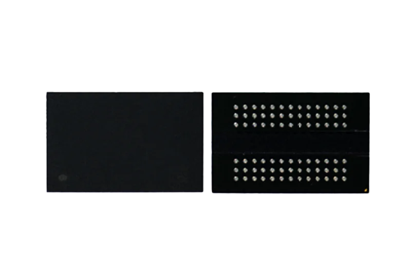
The Loongtion 8Gb DDR4 DRAM chip (1G×8 or 512M×16, 3200 MT/s) includes programmable On-Die Termination (ODT) with multiple RTT_NOM settings (RZQ/4, RZQ/2, RZQ/6, etc.) and dynamic ODT via RTT_WR, as detailed in the Loongtion 8Gb DDR4 DRAM chip whitepaper (Section 4.5 and Section 8.5). Debugging must verify that the selected ODT value actually provides the intended impedance match at both temperature extremes. Similarly, write leveling compensates for clock-to-strobe skew inherent in fly-by topology; if the controller's write leveling algorithm fails to train correctly at cold, the DQS edge may not be centered in the data eye.
VREF noise is another common issue. DDR4 uses internal VREF generation for command/address and data, but external VREF decoupling is still critical. A noisy VREF reduces the effective timing margin. Probing VREF with a low-capacitance active probe can reveal noise that the DRAM internal receiver sees.
Practical Probing Selection and Measurement Setup
Choosing the right probe depends on what you are measuring and where. The following table summarizes probe options and their suitability for DDR4 debug.
| Probe Type | Bandwidth | Loading | Best For | Caveat |
|---|---|---|---|---|
| 10× passive (short ground spring) | ≤500 MHz | ~10 pF, ~10 nH inductance | Low-speed signals: RESET_n, CKE, VREF | Too slow for DQS or data edges above 1 GHz |
| 1.75 GHz active single-ended | ≥1.75 GHz | ~0.5 pF, 1 MΩ | DQ, DM, address/command single-ended | Needs nearby ground via; may load weak ODT when RTT is high |
| 4 GHz differential active | ≥4 GHz | ~0.3 pF, 50 kΩ | DQS_t/DQS_c, CK_t/CK_c, differential clocks | Expensive; requires differential probe amplifier |
| Solder-in tips (resistive) | DC to >6 GHz | ~0.1 pF, 450 Ω | Attaching to fine-pitch BGA via test pad | Requires board re-spin with test points; acceptable attenuation |
For measuring DQS tCK and skew, a differential active probe with bandwidth at least 4 GHz is recommended. For checking DQ eye height and width, a single-ended active probe into a dedicated test pad is acceptable.
Setup workflow:
- Identify test points: Place 0201 or larger footprint pads on the backside of the board for each signal of interest, routed with a short stub to the main trace (length < 5 mm, impedance 50 Ω). Avoid via-to-via routing.
- Characterize the probe: Before attaching to the DUT, measure probe response using a known square wave from a fast pulse generator to de-skew the scope channels.
- Set up the oscilloscope: 50 Ω input, acquisition memory long enough to capture a full write burst (e.g., 10 μs at 40 GS/s). Use persistence mode to see worst-case jitter.
- Trigger: Use a DQS strobe or a clock signal as trigger. For write measurement, use the controller's command bus to trigger on a write command.
Probe calibration is often overlooked. The whitepaper (Section 8.6) emphasizes the need to account for probe loading in simulation vs. measurement. A solder-in resistive tip provides the most accurate representation because it minimizes capacitive loading and inductance. Always de-solder and re-solder the tip if the ground path appears inductive.
Debugging a Real-World Application Scenario – Write Leveling and DQS Skew on a 16-Layer Board
Note: The following scenario is illustrative, based on common field issues encountered by our application engineers.
Consider an industrial controller board with a Loongtion 8Gb DDR4 DRAM chip (×16 configuration, 3200 MT/s) on a 16-layer PCB. The board exhibits occasional write failures at –20°C after 30 minutes of operation. The system uses fly-by topology for the address/command bus.
Step 1: Measure CK_t/CK_c at the DRAM ball using a differential probe on a backside test pad. Look for crossing voltage level (typically VDD/2). At –20°C, the crossing may shift if the reference clock path has a DC offset or if the differential amplitude is low.
Step 2: Measure DQS_t/DQS_c during write leveling training. The controller should adjust DQS delay so that the rising edge of DQS aligns with the rising edge of CK at the DRAM. Probe both simultaneously on the scope. If the duty cycle distortion on DQS exceeds ±5%, write leveling may fail to lock.
Step 3: Check DQ to DQS timing alignment during a write burst. With a single-ended active probe on DQ[0] and differential probe on DQS, measure tDQSS (the DQS-to-CK setup time). The Loongtion 8Gb DDR4 DRAM chip specification requires tDQSS to be within a specified range for successful write (refer to the whitepaper for exact values). At –20°C, the propagation delay of the address/command bus may change differently than the data bus due to material Dk variation, causing tDQSS to drift out of spec.
Step 4: Measure VREF noise. With a 500 MHz bandwidth active probe, connect to the VREF pin on the DRAM. High-frequency ripple from DQ switching on the same package may couple into VREF, shrinking the data eye. If ripple > 20 mVpp, consider adding a 0.1 μF capacitor close to the VREF pin.
After adjusting ODT from RZQ/6 (40 Ω) to RZQ/4 (60 Ω) on MR1 and re-running write leveling training with a wider delay window, the failures disappeared. The new ODT better matched the PCB impedance at low temperature, reducing reflections that had been corrupting the DQ eye.
Simulation vs. Measurement Correlation
Simulation models often assume ideal probe loading without parasitic capacitance and inductance. Actual probe loading alters the measured waveform, especially for high-speed edges. To improve correlation, include a model of the probe in the simulation and compare against measurements using the same probe type. The Loongtion 8Gb DDR4 DRAM chip whitepaper provides guidance on this correlation in Section 8.6. A consistent approach between simulation and measurement reduces debug time and increases confidence in design margins.
Field Lessons – Common Pitfalls and Troubleshooting Workflow
| Symptom | Likely Cause | Probing Approach | Fix |
|---|---|---|---|
| Intermittent write failures at cold | Write leveling drift | Measure CK and DQS alignment at cold; check DQS duty cycle | Widen write leveling window; adjust ODT |
| Read errors at hot | ODT mismatch | Measure DQ eye height; check RTT_NOM | Increase RTT_NOM; add series resistor |
| Multiple-bit errors on same byte | VREF noise | Probe VREF during burst; look for ripple > 30 mV | Add bypass cap; move VREF trace away from DQ |
| Single-bit errors on random bits | Crosstalk on DQ | Probe victim DQ while aggressor is toggling | Reroute victim; increase spacing; reduce slew rate |
Field lesson: When probing on a live industrial board during temperature cycling, use a coaxial cable with a short (2 cm) ground wire soldered directly to a ground via. Avoid long ground leads. For differential signals, use a differential probe or two matched single-ended probes with mathematical subtraction to reject common-mode noise.
Another lesson: Always measure at both temperature corners. The Loongtion 8Gb DDR4 DRAM chip guarantees operation from –55°C to +105°C. The signal integrity margins narrow at extremes. A design that passes at 25°C may fail at –40°C due to increased rise time from higher trace resistance (copper resistivity increases about 0.4% per °C). Account for this in timing simulations.
Never rely solely on simulation; hardware probing is essential. Many simulation models assume ideal probe loading. Actual probe capacitance and inductance alter the measured waveform. Use solder-in tips (resistive) for the most accurate representation of the true signal.
Conclusion
Debugging DDR4 signal integrity on multi-layer industrial PCBs demands the right probing hardware, a systematic measurement approach, and an understanding of how temperature changes impact timing and impedance. By selecting differential active probes for clocks and strobes, using solder-in tips for fine-pitch test points, and measuring worst-case thermal conditions, you can identify and correct failures before production. The Loongtion 8Gb DDR4 DRAM chip provides the ODT flexibility and write leveling support needed to achieve robust signaling, but validating those features on your specific board layout is essential. For access to full electrical parameters and simulation models, consult the latest Loongtion 8Gb DDR4 DRAM chip datasheet or contact our application engineering team.
For related products and specifications, see the industrial memory chip product line.
By Loongtion Technical Team
Related products
Shortlist lines referenced in this guide — open the product page for PN, grades, and datasheet request.
Related resources
Continue with related selection guides and notes for the same industrial storage topic.
Related cross-references
Pin-to-pin and functional alternatives referenced from this guide — for BOM review, dual-sourcing, or EOL coverage.