
| Parameter | Specification |
|---|---|
| Industrial DDR3 SDRAM | JEDEC-compliant industrial memory with speed bins up to 2133 MT/s, DDR3/DDR3L voltage flexibility, and extended temperature operation to 105°C for long-life embedded platforms.s |
- JEDEC Compliant
- Industrial & Extended Temp
- −40°C to 85°C & −55°C to 105°C
- Up to 2133 MT/s
Ningbo Loongtion Intelligent Technology Co., Ltd.
hi@loongtion.com | www.loongtion.com
Document Version 2.2 | June 2026
1. Executive Summary
Ningbo Loongtion Intelligent Technology Co., Ltd. (Loongtion®) presents the Loongtion DDR3 SDRAM, a high-speed, JEDEC-compliant dynamic random-access memory component designed for demanding industrial, embedded, medical, and commercial applications. Built on a B-Die process, this memory device supports a wide range of speed bins from DDR3-800 to DDR3-2133, enabling system architects to select the optimal balance of performance and power consumption.
The Loongtion DDR3 SDRAM incorporates an 8-bank core architecture with 8n-bit prefetch, delivering burst-oriented read and write operations with data rates up to 2133 MT/s. The component is offered in both standard DDR3 (1.5 V nominal) and low-voltage DDR3L (1.35 V nominal) configurations, allowing seamless integration into power-sensitive designs. Available capacities of 2 Gb, 4 Gb, and 8 Gb with ×8 and ×16 data widths provide flexibility for a broad spectrum of memory subsystem requirements.
Key features include extended temperature ranges up to 105°C, comprehensive on-die termination (ODT) options including dynamic ODT, write leveling support for fly-by topology compensation, and self-calibration via an external ZQ resistor. These features, combined with robust DLL operation and multiple low-power modes, make the Loongtion DDR3 SDRAM a reliable choice for systems requiring domestically sourced memory with proven JEDEC compatibility.
2. Product Overview
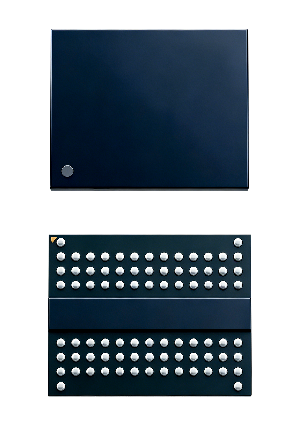
The Loongtion DDR3 SDRAM is a high-speed DRAM component manufactured on B-Die technology. It is designed to meet JEDEC standards and is available in speed bins from DDR3-800 through DDR3-2133. The device supports both ×8 and ×16 data width configurations, packaged in a compact 96-ball Fine-Pitch Ball Grid Array (FBGA) that is RoHS compliant and lead-free.
The following part numbers are currently offered, covering industrial and extended temperature ranges:
| Part Number | Capacity | Organization | Package | Temperature Range |
|---|---|---|---|---|
| YZ38E16SBB-9MFB-M(0) | 2 Gb | 128 Mb × 16 | 96-ball FBGA | −40°C to 85°C |
| YZ38E16SBB-9MFB-M | 2 Gb | 128 Mb × 16 | 96-ball FBGA | −55°C to 105°C |
| YZ38F16SBB-9MFD-M(0) | 4 Gb | 256 Mb × 16 | 96-ball FBGA | −40°C to 85°C |
| YZ38F16SBB-9MFD-M | 4 Gb | 256 Mb × 16 | 96-ball FBGA | −55°C to 105°C |
| YZ38G16SDB-9INN-M(0) | 8 Gb | 512 Mb × 16 | 96-ball FBGA | −40°C to 85°C |
*Note: Part numbers for ×8 configurations are not specified in source documentation.*
The supported speed bins include DDR3-800, DDR3-1066, DDR3(L)-1066, DDR3-1333, DDR3(L)-1333, DDR3(L)-1600, DDR3(L)-1866, and DDR3-2133. The "(L)" notation indicates devices validated for both DDR3 (1.5 V) and DDR3L (1.35 V) operation. The document revision history spans from Rev 1.0 (2022/05) to Rev 2.2 (2026/5).
3. Technology and Architecture
3.1 Core Architecture
The Loongtion DDR3 SDRAM employs an 8-bank DRAM core with an 8n-bit prefetch DDR architecture. A single read or write operation accesses an 8n-byte-wide data block, with data transferred in four clock cycles at the DRAM core and four clock cycles at the I/O pins. Read and write operations are burst-oriented, starting at a selected location and proceeding sequentially or interleaved as programmed.
3.2 Clock and Strobe Architecture
All control and address inputs are synchronized with a pair of external differential clocks (CK, CK#). Inputs are sampled at the crossing point of the differential clock—the rising edge of CK and the falling edge of CK#. All I/Os are synchronized in a source-synchronous manner using either a single-ended DQS signal or a differential DQS pair. The bidirectional differential data strobe (DQS, DQS#) aligns with data during reads (edge-aligned) and writes (center-aligned). An on-chip PLL ensures alignment between CK and the data signals DQ, DQS, and DQS#. The interface enables each I/O pin to transfer two words per clock cycle.
3.3 Command Protocol
All address and control input signals except data, data strobe, and data mask are latched on the rising edge of CK. The device supports a full command set including Activate, Precharge, Mode Register Set (MRS), Refresh, Self-Refresh Entry/Exit, ZQ Calibration (Long and Short), Reset, Multi-Purpose Register (MPR) access, and various Read and Write commands with burst length options (fixed BC4, fixed BL8, or on-the-fly).
3.4 DLL Operation
The Delay-Locked Loop (DLL) must be enabled for normal operation (MR1 bit A0 = 0). The DLL is automatically disabled during self-refresh and automatically re-enabled upon exit. After a DLL reset, the system must wait tDLLK clock cycles before issuing a read or synchronous ODT command. The DDR3 SDRAM does not require the DLL for any write operation except when RTT_WR is enabled and ODT operation requires DLL support. Two precharge power-down DLL modes are available: slow exit (freezes DLL to save power) and fast exit (keeps DLL active), selected via MR0 bit A12.
3.5 Mode Registers
Four programmable mode registers provide extensive configuration flexibility:
| Register | Address Bits (BA[2:0]) | Key Functions |
|---|---|---|
| MR0 | 000 | Burst length (BL=4 or 8), read burst type (sequential/interleaved), CAS latency (CL=5–16), write recovery (WR=5–16), DLL reset, test mode, precharge power-down DLL control |
| MR1 | 001 | DLL enable/disable, output driver strength (RZQ/6 or RZQ/7), Rtt_Nom impedance (120 Ω, 60 Ω, 40 Ω, 30 Ω, 20 Ω, or disabled), additive latency (AL=0 to CL-2), write leveling enable, TDQS enable, Qoff |
| MR2 | 010 | CAS write latency (CWL=5–12), auto self-refresh (ASR), self-refresh temperature (SRT), Rtt_WR (dynamic ODT) |
| MR3 | 011 | Multi-purpose register (MPR) mode and location |
When programming mode registers, all address fields within the accessed mode register must be redefined, even if only a subset of MRS fields is being modified. Reserved for Future Use (RFU) bits must be programmed to 0.
3.6 Additive Latency
Additive latency (AL) allows a read or write command to be issued immediately after an activate command; the command is held internally for AL cycles before being issued. Read latency (RL) equals AL plus CAS latency (CL). Write latency (WL) equals AL plus CAS write latency (CWL). The DDR3 DRAM does not support half-clock latency.
3.7 Self-Calibration
The device performs self-calibration via the ZQ pin, which requires an external resistor RZQ = 240 Ω ± 1%. Two calibration commands are supported: ZQCL (long calibration) performs initial calibration during the power-up initialization sequence, and ZQCS (short calibration) performs periodic calibration to compensate for voltage and temperature variations. Before issuing ZQCL or ZQCS, all banks must be precharged and tRP timing satisfied. In systems with shared ZQ resistors, the controller must not allow overlap of tZQoper, tZQinit, or tZQCS timing between ranks.
4. Key Features and Differentiators
4.1 Wide Voltage and Speed Range
The Loongtion DDR3 SDRAM supports both DDR3 (VDD = VDDQ = 1.5 V nominal) and DDR3L (1.35 V nominal) operation on the same device, with VDD and VDDQ driven by a single power supply. A broad speed spectrum from 800 MT/s to 2133 MT/s enables designers to match performance requirements without over-provisioning.
4.2 Extended Temperature Operation
Two temperature grades are available:
- Industrial Temperature Range: −40°C to 85°C (part numbers with (0) suffix)
- Extended Temperature Range: −55°C to 105°C (part numbers without suffix)
IDD current derating guidelines ensure reliable operation at elevated temperatures: all IDD values must be increased by 30% when case temperature (Tc) exceeds 95°C, and by 50% when Tc exceeds 105°C. Self-refresh mode is not available above 105°C.
4.3 On-Die Termination (ODT)
The device provides comprehensive ODT support with both synchronous and dynamic modes:
- RTT_Nom: Programmable via MR1 bits A[9,6,2] to values of RZQ/4 (60 Ω), RZQ/2 (120 Ω), RZQ/6 (40 Ω), RZQ/12 (20 Ω), RZQ/8 (30 Ω), or disabled
- RTT_WR: Programmable via MR2 bits A[10,9] to RZQ/4 or RZQ/2, enabled in dynamic ODT mode
- ODT latencies: ODTLon = WL − 2; ODTLoff = WL − 2 (synchronous mode)
4.4 Write Leveling
To compensate for propagation time skew between the clock and data strobe caused by fly-by topology, the device supports a write leveling function. Write leveling mode is entered by setting MR1 bit 7 HIGH and exited by setting it LOW. During write leveling, DQS and DQS# terminations are enabled/disabled via the ODT pin, differing from normal operation.
4.5 TDQS (Termination Data Strobe)
For ×8 configurations, the TDQS feature provides additional termination resistor functionality. When TDQS is enabled, the DM function is not supported. In ×16 configurations, TDQS must be disabled via MR1 with A11 = 0.
4.6 Low-Power Modes
Multiple power-saving states are available:
- Precharge Power-Down: Slow exit (freezes DLL) or fast exit (DLL active)
- Active Power-Down
- Self-Refresh: Normal mode (IDD6 = 25 mA) and Extended Temperature mode (IDD6ET = 28 mA)
4.7 Multi-Purpose Register (MPR)
The MPR allows the system to read a predefined calibration pattern for timing training. When enabled via MR3 A2 = 1, all DQ pins output the same single-bit data in BL8 mode. The DLL must be locked before an MPR read operation.
5. Technical Specifications
5.1 Package Dimensions (96-ball FBGA)
| Parameter | Min (mm) | Nom (mm) | Max (mm) |
|---|---|---|---|
| A (height) | Not specified | 1.12 | 1.20 |
| A1 | 0.73 | 0.78 | 0.83 |
| A2 | 0.30 | 0.35 | 0.40 |
| D (length) | 8.90 | 9.00 | 9.10 |
| E (width) | 12.90 | 13.00 | 13.10 |
| D1 | 6.30 | 6.40 | 6.50 |
| E1 | 11.90 | 12.00 | 12.10 |
| W | — | — | 2.00 |
| t (thickness) | 0.10 | 0.15 | 0.20 |
| e (ball pitch) | — | 0.80 | — |
| d | — | 0.80 | — |
| b (ball diameter) | 0.40 | 0.45 | 0.50 |
5.2 Supply Voltages
| Parameter | DDR3 | DDR3L |
|---|---|---|
| VDD = VDDQ (Nominal) | 1.5 V | 1.35 V |
| VDD = VDDQ (Min) | 1.425 V | 1.282 V |
| VDD = VDDQ (Max) | 1.575 V | 1.45 V |
- VDD and VDDQ must be within 300 mV of each other at all times.
- Under all conditions, VDDQ must be less than or equal to VDD.
- When both VDD and VDDQ are less than 500 mV, Vref must be no greater than 0.6 × VDDQ.
- Vref = VDDQ/2.
- VTT is limited to a maximum of 0.95 V after power supply voltage ramp-up is complete.
- Power supply ramp time between 300 mV and minimum VDD must be within 200 ms.
5.3 Absolute Maximum Ratings
| Parameter | Min | Max |
|---|---|---|
| Voltage on VDD pin relative to VSS | −0.4 V | 1.8 V |
| Voltage on VDDQ pin relative to VSS | −0.4 V | 1.8 V |
| Voltage on input/output pins relative to VSS | −0.4 V | 1.8 V |
| Storage temperature (TSTG) | −55°C | 100°C |
| Absolute maximum junction temperature (Tj max) | — | 125°C |
5.4 Thermal Characteristics
| Parameter | Value |
|---|---|
| Thermal resistance | 28.3°C/W |
5.5 IDD Current Specifications (×8 Configuration)
| Parameter | DDR3-1600 | DDR3-1866 | DDR3-2133 |
|---|---|---|---|
| IDD0 (One Bank Active → Precharge) | 100 mA | 120 mA | 130 mA |
| IDD1 (One Bank Active → Read → Precharge) | 110 mA | 125 mA | 135 mA |
| IDD2P0 (Precharge Power Down Slow Exit) | 20 mA | 20 mA | 20 mA |
| IDD2P1 (Precharge Power Down Fast Exit) | 43 mA | 45 mA | 47 mA |
| IDD2Q (Precharge Quiet Standby) | 58 mA | 63 mA | 68 mA |
| IDD2N (Precharge Standby) | 61 mA | 66 mA | 71 mA |
| IDD2NT (Precharge Standby ODT) | 83 mA | 90 mA | 96 mA |
| IDD3N (Active Standby) | 88 mA | 96 mA | 100 mA |
| IDD3P (Active Power-Down) | 68 mA | 77 mA | 82 mA |
| IDD4R (Burst Read) | 180 mA | 210 mA | 230 mA |
| IDD4W (Burst Write) | 200 mA | 240 mA | 265 mA |
| IDD5B (Burst Refresh) | 170 mA | 185 mA | 200 mA |
| IDD6 (Self Refresh Normal) | 25 mA | 25 mA | 25 mA |
| IDD6ET (Self Refresh Extended) | 28 mA | 28 mA | 28 mA |
| IDD7 (All Bank Interleave Read) | 220 mA | 255 mA | 275 mA |
| IDD8 (Reset Low) | 21 mA | 21 mA | 22 mA |
5.6 IDD Current Specifications (×16 Configuration)
| Parameter | DDR3-1600 | DDR3-1866 | DDR3-2133 |
|---|---|---|---|
| IDD0 | 110 mA | 130 mA | 150 mA |
| IDD1 | 120 mA | 135 mA | 155 mA |
| IDD2P0 | 22 mA | 22 mA | 22 mA |
| IDD2P1 | 45 mA | 47 mA | 47 mA |
| IDD2Q | 60 mA | 65 mA | 70 mA |
| IDD2N | 63 mA | 68 mA | 73 mA |
| IDD2NT | 85 mA | 92 mA | 98 mA |
| IDD3N | 90 mA | 100 mA | 105 mA |
| IDD3P | 70 mA | 80 mA | 85 mA |
| IDD4R | 190 mA | 220 mA | 240 mA |
| IDD4W | 210 mA | 250 mA | 280 mA |
| IDD5B | 180 mA | 195 mA | 210 mA |
| IDD6 | 25 mA | 25 mA | 25 mA |
| IDD6ET | 28 mA | 28 mA | 28 mA |
| IDD7 | 240 mA | 270 mA | 290 mA |
| IDD8 | 23 mA | 23 mA | 24 mA |
5.7 Capacitance Parameters
| Parameter | DDR3-1066 | DDR3-1333 | DDR3-1600 | DDR3-1866 | DDR3-2133 |
|---|---|---|---|---|---|
| CIO (DQ, DM, DQS, DQS#, TDQS, TDQS#) | 1.2–2.7 pF | 1.2–2.5 pF | 1.2–2.3 pF | 1.2–2.2 pF | 1.2–2.1 pF |
| CCK (CK, CK#) | 0.6–1.6 pF | 0.6–1.4 pF | 0.6–1.4 pF | 0.6–1.3 pF | 0.6–1.3 pF |
| CDCK (CK, CK# delta) | 0–0.15 pF | 0–0.15 pF | 0–0.15 pF | 0–0.15 pF | 0–0.15 pF |
| CDDOS (DQS, DQS# delta) | 0–0.2 pF | 0–0.15 pF | 0–0.15 pF | 0–0.15 pF | 0–0.15 pF |
| CI (CTRL, ADD, CMD) | 0.55–1.35 pF | 0.55–1.3 pF | 0.55–1.3 pF | 0.55–1.2 pF | 0.55–1.2 pF |
| CDI_CTRL | −0.5 to 0.3 pF | −0.4 to 0.2 pF | −0.4 to 0.2 pF | −0.4 to 0.2 pF | −0.4 to 0.2 pF |
| CDI_ADD_CMD | −0.5 to 0.5 pF | −0.4 to 0.4 pF | −0.4 to 0.4 pF | −0.4 to 0.4 pF | −0.4 to 0.4 pF |
| CDIO (DQ, DM, DQS, DQS#, TDQS, TDQS#) | −0.5 to 0.3 pF | −0.5 to 0.3 pF | −0.5 to 0.3 pF | −0.5 to 0.3 pF | −0.5 to 0.3 pF |
| CZQ (ZQ) | 3 pF | 3 pF | 3 pF | 3 pF | 3 pF |
*Capacitance measured per JEP147 with VDD = VDDQ = 1.5 V, VBIAS = VDD/2, on-die termination disabled. Maximum external load capacitance on ZQ pin: 5 pF.*
5.8 Speed Bin Timing Parameters
| Speed Bin | CL-nRCD-nRP | tAA (min) | tRCD (min) | tRP (min) | tRAS (min) | tRC (min) |
|---|---|---|---|---|---|---|
| DDR3-2133 | 14-14-14 | 13.09 ns | 13.09 ns | 13.09 ns | 33 ns | 40.09 ns |
| DDR3(L)-1866 | 13-13-13 | 13.91 ns | 13.91 ns | 13.91 ns | 34 ns | 47.91 ns |
| DDR3(L)-1600 | 11-11-11 | 13.75 ns | 13.75 ns | 13.75 ns | 35 ns | 48.75 ns |
| DDR3(L)-1333 | 9-9-9 | 13.5 ns | 13.5 ns | 13.5 ns | 36 ns | 49.5 ns |
| DDR3-1333 | 10-10-10 | 15 ns | 15 ns | 15 ns | 36 ns | 51 ns |
| DDR3(L)-1066 | 7-7-7 | 13.125 ns | 13.125 ns | 13.125 ns | 37.5 ns | 50.625 ns |
| DDR3-1066 | 8-8-8 | 15 ns | 15 ns | 15 ns | 37.5 ns | 52.5 ns |
- tRAS max = 9 × tREFI for all speed bins.
- tAA max = 20 ns for all speed bins.
- Supported CL values: 5, 6, 7, 8, 9, 10, 11, 12, 13, 14.
- Supported CWL values: 5, 6, 7, 8, 9, 10, 11, 12.
5.9 REF Command to ACT or REF Command Time (tRFC)
| Density | tRFC |
|---|---|
| 1 Gb | 110 ns |
| 2 Gb | 160 ns |
| 4 Gb | 260 ns |
| 8 Gb | 350 ns |
5.10 CAS Write Latency (CWL) Timing Ranges
| CWL | tCK Range |
|---|---|
| 5 | tCK ≥ 2.5 ns |
| 6 | 2.5 ns > tCK ≥ 1.875 ns |
| 7 | 1.875 ns > tCK ≥ 1.5 ns |
| 8 | 1.5 ns > tCK ≥ 1.25 ns |
| 9 | 1.25 ns > tCK ≥ 1.07 ns |
| 10 | 1.07 ns > tCK ≥ 0.935 ns |
| 11 | 0.935 ns > tCK ≥ 0.833 ns |
| 12 | 0.833 ns > tCK ≥ 0.75 ns |
6. Performance and Reliability
6.1 Speed Grade Summary
| Speed Grade | CL | tCK(min) | tRCD(min) | tRP(min) | tRAS(min) | tRC(min) |
|---|---|---|---|---|---|---|
| DDR3-800 | 6 | 2.5 ns | 15 ns | 15 ns | 37.5 ns | 52.5 ns |
| DDR3-1066 | 7 | 1.875 ns | 13.125 ns | 13.125 ns | 37.5 ns | 50.625 ns |
| DDR3-1333 | 9 | 1.5 ns | 13.5 ns | 13.5 ns | 36 ns | 49.5 ns |
| DDR3-1600 | 11 | 1.25 ns | 13.75 ns | 13.75 ns | 35 ns | 48.75 ns |
| DDR3-1866 | 13 | 1.071 ns | 13.91 ns | 13.91 ns | 34 ns | 47.91 ns |
| DDR3-2133 | 14 | 0.938 ns | 13.09 ns | 13.09 ns | 33 ns | 46.09 ns |
6.2 Lower Frequency Support and Down Binning
Each speed grade supports functional operation at lower frequencies. When the DRAM data rate is lower than 800 MT/s, DDR3-800 AC timing applies. For devices supporting optional down bin configurations (e.g., to CL=7 or CL=9), tAAmin, tRCDmin, and tRPmin must be 13.125 ns, and the Serial Presence Detect (SPD) must be programmed accordingly.
6.3 Burst Performance
Burst read and write operations support lengths of 4 or 8 (fixed or on-the-fly selectable) in sequential or interleaved modes. Burst operations cannot be terminated or interrupted once initiated.
6.4 Refresh and Self-Refresh
The device supports normal self-refresh (IDD6 = 25 mA across all speed grades) and extended temperature self-refresh (IDD6ET = 28 mA). When the case temperature exceeds 105°C, refresh is required; self-refresh mode is not available under these conditions. IDD temperature derating is mandatory: all IDD values must be increased by 30% when Tc > 95°C and by 50% when Tc > 105°C.
6.5 Calibration and DLL Reliability
Initial ZQ calibration (ZQCL) ensures output driver and ODT accuracy. Periodic ZQCS commands compensate for voltage and temperature drift. The DLL must be locked before read operations or synchronous ODT commands, with tDLLK wait time enforced after DLL reset.
7. Applications and Target Markets
The Loongtion DDR3 SDRAM is designed for a wide variety of systems requiring reliable, domestically sourced memory with industrial-grade robustness.
| Market Segment | Typical Applications | Key Requirements Met |
|---|---|---|
| Industrial Automation | PLCs, HMIs, motor drives | Extended temperature, robust power supply tolerance |
| Embedded Systems | Single-board computers, networking equipment, IoT gateways | Compact 96-ball FBGA, wide speed/voltage options |
| Medical Equipment | Patient monitors, diagnostic imaging, infusion pumps | Industrial temperature range, high reliability |
| Commercial Systems | Thin clients, POS terminals, digital signage | High bandwidth up to 2133 MT/s, low power |
| Aerospace / Defense | Ruggedized computing, avionics | Extended temperature (−55°C to 105°C) capabilities |
8. System Integration and Design Considerations
8.1 Fly-By Topology and Write Leveling
The DDR3 SDRAM uses a fly-by topology for command, address, control signals, and clocks. To compensate for propagation time skew between the clock and data strobe that results from this topology, the system must enable write leveling (MR1 bit 7 = 1). During write leveling, only DQS and DQS# terminations are controlled via the ODT pin, which differs from normal operation.
8.2 ODT Configuration Guidelines
- ODT input signals are in a don't-care state during tIS cycles until CKE is registered HIGH.
- When CKE is HIGH, ODT signals can be statically held HIGH or LOW. If RTT_NOM is enabled, ODT must be held LOW.
- During read operations, ODT must be disabled externally.
- Dynamic ODT mode is enabled via MR2 bits A9 or A10. In this mode, RTT_Nom is selected during operations without a write command; when a write command is registered, after ODTLcnw clock cycles, RTT_WR is selected.
- ODT is not available during DLL Off mode or self-refresh mode.
8.3 Power Sequencing
- VDD and VDDQ must ramp from 300 mV to minimum operating voltage within 200 ms.
- During ramp: VDD > VDDQ and (VDD − VDDQ) < 0.3 V.
- After ramp completion, VTT is limited to a maximum of 0.95 V.
- Voltage levels on all pins except VDD, VDDQ, VSS, and VSSQ must be ≤ VDD and VDDQ, and ≥ VSS and VSSQ.
8.4 ZQ Resistor Routing
The ZQ pin requires an external 240 Ω ± 1% resistor. In multi-rank systems with a shared ZQ resistor, the controller must ensure that tZQoper, tZQinit, and tZQCS timing intervals do not overlap between ranks.
8.5 CKE and Self-Refresh
CKE must be registered with the same value on consecutive positive clock edges for tCKEmin. Self-refresh exit is asynchronous; Vref (VrefDQ and VrefCA) must be maintained during self-refresh. Input clock frequency can be changed only in self-refresh mode or precharge power-down mode.
8.6 DLL and Frequency Changes
Any frequency change must be performed while in self-refresh or precharge power-down. During a frequency change in precharge power-down, ODT and CKE must remain stable low. After exiting precharge power-down, the DLL must be reset via an MRS command.
8.7 Mode Register Programming
When programming any mode register, all address fields within the accessed mode register must be redefined, even if only a subset of MRS fields is being modified. RFU bits must be programmed to 0.
8.8 Drive Strength Selection
The output driver impedance is defined by the external reference resistor RZQ (240 Ω ± 1%). Two settings are available: R (nominal 34.4 Ω ± 10%) and R (nominal 40 Ω). Mismatch between pull-up and pull-down at VOMdc = 0.5 × VDDQ is within −10% to +10%.
8.9 Capacitance and Loading Considerations
The capacitance values provided in Section 5.7 should be used for signal integrity analysis. The maximum external load capacitance on the ZQ pin is 5 pF.
9. Standards Compliance and Quality
The Loongtion DDR3 SDRAM is designed and manufactured in accordance with JEDEC standards. Key compliance characteristics include:
- JEDEC Standard Package: 96-ball FBGA (Fine-Pitch Ball Grid Array) per JEDEC specification.
- RoHS Compliance: The device is lead-free and RoHS compliant.
- Temperature Grades: Industrial (−40°C to 85°C) and extended (−55°C to 105°C) as specified in part numbers.
- Absolute Maximum Ratings: Storage temperature −55°C to 100°C; maximum junction temperature 125°C.
- ZQ Calibration: Uses external 240 Ω ± 1% resistor per JEDEC.
- Signal Integrity: DC and AC input levels, differential crosspoint voltages, and output levels meet JEDEC requirements for all supported speed grades.
- Documentation: Datasheet revisions include Rev 1.0 (2022/05) through Rev 2.2 (2026/5).
Quality assurance measures include characterization and design verification for lower-frequency operation across all speed grades, as well as mandatory IDD derating guidelines for operation above 95°C.
10. Ordering Information
The following part numbers are available for the Loongtion DDR3 SDRAM:
| Part Number | Capacity | Organization | Package | Temperature Range |
|---|---|---|---|---|
| YZ38E16SBB-9MFB-M(0) | 2 Gb | 128 Mb × 16 | 96-ball FBGA | −40°C to 85°C |
| YZ38E16SBB-9MFB-M | 2 Gb | 128 Mb × 16 | 96-ball FBGA | −55°C to 105°C |
| YZ38F16SBB-9MFD-M(0) | 4 Gb | 256 Mb × 16 | 96-ball FBGA | −40°C to 85°C |
| YZ38F16SBB-9MFD-M | 4 Gb | 256 Mb × 16 | 96-ball FBGA | −55°C to 105°C |
| YZ38G16SDB-9INN-M(0) | 8 Gb | 512 Mb × 16 | 96-ball FBGA | −40°C to 85°C |
Temperature Suffix: Part numbers with "(0)" indicate the industrial temperature range (−40°C to 85°C). Part numbers without "(0)" indicate the extended temperature range (−55°C to 105°C).
*Note: Additional part numbers for ×8 configurations are not specified in source documentation.*
11. About Loongtion
Ningbo Loongtion Intelligent Technology Co., Ltd. (Loongtion®) is a China-based developer and supplier of memory and solid-state storage products for industrial, embedded, medical, and commercial applications. The company's product portfolio includes:
- DDR3 / DDR4 / DDR5 SDRAM – Memory components for diverse computing platforms.
- LPDDR4X SDRAM – Low-power memory for mobile and embedded systems.
- eMMC 5.1 – Embedded multimedia card storage.
- M.2 NVMe SSD – High-performance solid-state drives.
- NVMe BGA SSD – Compact ball-grid-array solid-state storage solutions.
Loongtion focuses on providing domestically sourced memory and storage solutions that meet the rigorous demands of industrial and embedded environments. The company offers comprehensive technical support and long-term product availability.
Contact Information:
- Email: hi@loongtion.com
- Website: www.loongtion.com
Disclaimer: The specifications, features, and parameters included in this whitepaper are based solely on the consolidated fact sheet provided. For complete design-in information, refer to the latest official Loongtion datasheet. Specifications are subject to change without notice. Ningbo Loongtion Intelligent Technology Co., Ltd. assumes no liability for errors or omissions.
Related products
Shortlist lines referenced in this guide — open the product page for PN, grades, and datasheet request.
Related resources
Continue with related selection guides and notes for the same industrial memory topic.
Related cross-references
Pin-to-pin and functional alternatives referenced from this guide — for BOM review, dual-sourcing, or EOL coverage.