
A Systematic Debugging Workflow for DDR4 Signal Integrity Issues in Industrial PCB Designs
1. Verify Power Integrity Before SI
Measure VDD (1.2 V) and VPP (2.5 V) at the DRAM package pins. The Loongtion DDR4 specification (Section 5.1) allows ±5% on VDD and ±5% on VPP. Ripple must be below the JEDEC limits (typically 50 mV p-p). If ripple exceeds 100 mV, add decoupling capacitors near the balls. Use a 1:1 probe with a short ground spring—not a long ground lead—to avoid measuring false ripple.
2. Check ODT Settings
Read the current ODT settings via MRS read (MR1 for RTT_NOM, MR2 for RTT_WR). Compare to the target trace impedance. If the ODT is disabled or set too high (e.g., 120 Ω on a 45 Ω trace), expect reflections. A quick test: program RTT_NOM to a lower impedance setting (such as RZQ/5 = 48 Ω) and observe if error rate drops. The whitepaper's Section 8.5 provides detailed ODT configuration guidelines.
3. Validate Write Leveling
Use the controller’s write leveling feedback. If the leveling results are near the boundary of the allowed window (typically ±1 UI), the margin is low. Manually sweep the DQS delay in small steps (e.g., 10 ps) and measure the write eye using a write-leveling pattern (e.g., DQ = 0x55). The passing region should be at least 0.5 UI wide. If not, possible causes: unbalanced via count or excessive stub length.
4. Enable CA Parity and Write CRC
Program MR5 to enable CA parity (even parity) with the appropriate latency mode. On the host side, log any CA parity errors. Similarly, enable write CRC via MR2. If the controller reports CRC errors only on writes to specific byte lanes, suspect a weak DQS timing for that lane. If CRC errors are random across all lanes, suspect power supply noise or common-mode clock jitter. Refer to Sections 4.2 and 4.3 of the whitepaper for feature details.
5. Measure DQ/DQS Eye Diagram
Probe a DQ signal near the DRAM ball (do not probe at the controller—the far end shows the actual margin). With a repetitive read pattern (e.g., walking ones), capture the eye. Compare to the receiver mask in the DDR4 specification. If the eye height is less than 200 mV or width less than 0.4 UI, start reducing crosstalk by separating aggressor lines or increasing spacing to 3× the dielectric height.
6. Temperature Stress Test
Run the system in a thermal chamber with a custom script that writes and verifies all address locations. Cycle between –40°C and +85°C with a 5°C/min ramp. Monitor CA parity and CRC errors in real time. If errors appear only above 75°C, the issue may be timing drift due to DLL propagation delay change. Try increasing the CAS latency by one (from CL=22 to CL=24 at 3200 MT/s) and re-run.
Common Debugging Observations from Industrial Deployments
Observation 1: ODT mismatch is a frequent cause of intermittent fails. In some industrial HMI designs, field returns have shown data corruption during high-temperature operation. When ODT settings were adjusted to better match the trace impedance (e.g., using a 48 Ω setting instead of 40 Ω), errors were eliminated. Even a small reflection coefficient can degrade eye closure enough to cause setup violations at temperature.
Observation 2: VREF calibration can help recover margin. While Loongtion DDR4 does not require VREFDQ training (the device uses internal VREF generation; see Section 8.3), ensuring that the controller sets VREF to 0.5*VDDQ is important. If the internal VREF is within specification, margin is usually adequate. In some systems, manually verifying VREF at the DRAM pin can reveal drift due to PCB voltage drop.
Observation 3: Via stubs add deterministic jitter. Industrial PCBs often have thick cores (≥1.6 mm), resulting in via stubs of 0.8–1.2 mm on inner-layer transitions. Backdrilling is expensive but can be partially mitigated by keeping signal layers close to the surface. In practice, a 1.0 mm stub on a DQS line can reduce eye opening by 25% at 3200 MT/s. Write leveling can compensate for some skew, but jitter remains.
Observation 4: Use CA parity logs to distinguish board from DRAM faults. If CA parity errors are persistent on a specific command, the controller-driver or trace may have a high-resistance short. If errors are correlated with temperature but not with specific commands, the DRAM’s input receiver may be marginal. Loongtion’s CA parity (Section 4.2) logs the error so you can separate these cases without needing a scope.
Conclusion
DDR4 signal integrity debugging need not be a black art. By following a structured workflow—starting with power integrity, verifying ODT and write leveling, enabling built-in diagnostic features like CA parity and write CRC, and performing temperature stress tests—engineers can isolate the root cause in days rather than weeks. Loongtion’s industrial DDR4 chips, with their programmable ODT, extended temperature ranges, and error-detection capabilities, provide the instrumentation needed to debug and ultimately prevent SI failures in harsh environments. For designs requiring further analysis, consult the latest Loongtion DDR4 whitepaper for detailed ODT configuration tables and timing derating curves.
For related products and specifications, see the Industrial Memory Chips product line.
By Loongtion Technical Team
Related products
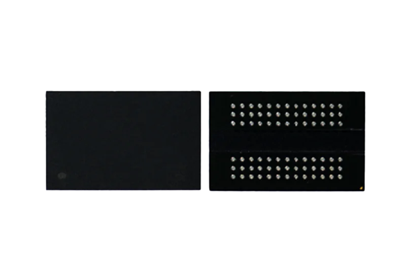
Shortlist lines referenced in this guide — open the product page for PN, grades, and datasheet request.
Related resources
Continue with related selection guides and notes for the same industrial storage topic.
Related cross-references
Pin-to-pin and functional alternatives referenced from this guide — for BOM review, dual-sourcing, or EOL coverage.