
| Parameter | Specification |
|---|---|
| Industrial NVMe BGA SSD | Compact BGA291 surface-mount NVMe with dual TLC/pSLC modes and HMB architecture, enabling rugged, space-constrained embedded integration without onboard DRAM. |
- JEDEC Compliant
- Industrial & Extended Temp
- −40°C to 85°C & −55°C to 105°C
- 32-512GB
Ningbo Loongtion Intelligent Technology Co., Ltd.
hi@loongtion.com | www.loongtion.com
Document Version 2.2 | June 2026
1. Executive Summary
The Loongtion NVMe BGA SSD is a fully China-domestic solid-state storage solution designed for embedded, industrial, and ruggedized applications requiring high reliability, wide temperature tolerance, and supply chain independence. This product integrates a proprietary Loongtion NVMe controller with Yangtze Memory TLC NAND Flash in a compact BGA291 package (20 mm × 16 mm × ~1.3 mm, weight <10 g). It operates over PCIe 3.0 using the NVMe 1.4 protocol, supports both native TLC (Triple-Level Cell) and pseudo-SLC (pSLC) modes, and employs a local-DRAM-less architecture with Host Memory Buffer (HMB) to reduce BOM cost and power consumption.
Key capabilities include:
- Dual-mode operation: TLC for capacity-optimized storage (256 GB, 512 GB) or pSLC for enhanced endurance and performance (32 GB, 64 GB, 128 GB).
- Industrial temperature grade: –40 °C to +85 °C; wide/military grade: –55 °C to +105 °C (screened parts).
- Low power consumption: As low as 1.6 W (pSLC read) and up to 3.1 W (TLC write).
- Performance envelope: Sequential read up to 1200 MB/s (pSLC), 4 KB random write up to 120 K IOPS; total bytes written (TBW) up to 600 TB in pSLC mode.
- Built-in protection features: Smart erase, power-loss notification, secure erase trigger, intelligent thermal throttling, and multiple data encryption mechanisms.
Target applications include embedded systems, industrial controllers, ruggedized computers, avionics, aerospace, defense, and marine electronics. The product is available in five standard capacities with two temperature grades, as detailed in Section 10 (Ordering Information).
Disclaimer: Specifications may change due to product version upgrades or other requirements. Users should refer to the latest official datasheet from Ningbo Loongtion Intelligent Technology Co., Ltd. for current and complete technical information.
2. Product Overview
The Loongtion NVMe BGA SSD is a member of the Loongtion solid-state storage product family, which spans DRAM modules, eMMC, and M.2 NVMe SSDs. It is offered in a BGA291 surface-mount package, enabling direct PCB integration for space-constrained designs.
Capacities and Operating Modes
| Nominal Capacity | Actual Capacity | Operating Mode | Interface | PCIe Lane Configuration |
|---|---|---|---|---|
| 32 GB | 29 GB | pSLC | PCIe 3.0 ×2, NVMe 1.4 | ×2 |
| 64 GB | 59 GB | pSLC | PCIe 3.0 ×2, NVMe 1.4 | ×2 |
| 128 GB | 119 GB | pSLC | PCIe 3.0 ×2, NVMe 1.4 | ×2 |
| 256 GB | 238 GB | TLC | PCIe 3.0 ×4, NVMe 1.4 | ×4 |
| 512 GB | 476 GB | TLC | PCIe 3.0 ×4, NVMe 1.4 | ×4 |
*Note: Actual capacity reflects formatted user capacity after overhead.*
Key Design Features
- Controller: China-domestic NVMe controller.
- NAND Flash: Yangtze Memory 3D TLC NAND.
- DRAM‑less architecture: No onboard DRAM; mapping tables reside in Host Memory Buffer (HMB) over PCIe.
- Dual-mode support: Same hardware can be configured for TLC (native) or pSLC (emulated, higher endurance and performance).
- Built-in Power-On Reset (POR) and intelligent thermal throttling.
- Multiple GPIO functions for system integration: secure erase (GP2), alert (GP3), LED status (GP4), power-loss handshake (GP7/GP8).
- Debug and management interfaces: I2C/SMBus, UART, JTAG.
Document Revision History
The product specification has evolved from V1.0 (2023.01.04) to V2.1 (2026.01.23), with a separate Hardware Design Guide at V2.2 (2026.01.23). The contents in this whitepaper reflect information from these latest versions.
3. Technology and Architecture
3.1 Controller Architecture
The Loongtion NVMe BGA SSD uses a proprietary China-domestic NVMe controller compliant with the NVMe 1.4 specification. The host interface is PCIe 3.0, supporting up to four lanes in TLC mode (×4) or two lanes in pSLC mode (×2). The controller implements a local-DRAM-less design; all memory-mapped table data is stored in the host’s system memory via the Host Memory Buffer (HMB) feature defined in NVMe 1.4. This reduces component count, BOM cost, and board space.
3.2 NAND Flash and Dual-Mode Operation
The storage medium is Yangtze Memory 3D TLC NAND. The controller supports two modes of operation:
- TLC (Triple-Level Cell) mode: Each cell stores three bits, optimizing for capacity. Used in 256 GB and 512 GB SKUs.
- pSLC (pseudo-Single-Level Cell) mode: The controller emulates SLC behavior by programming each TLC cell with only one bit. This provides higher write endurance, lower latency, and better performance at the cost of reduced effective capacity. Used in 32 GB, 64 GB, and 128 GB SKUs.
The boot-up or firmware‑configurable mode selection allows the same hardware platform to address either capacity- or endurance-oriented requirements.
3.3 Power Architecture
The SSD requires multiple supply rails:
| Supply Rail | Min | Typ | Max | Ripple Noise | Guaranteed Current |
|---|---|---|---|---|---|
| VCC | 2.97 V | 3.3 V | 3.63 V | ≤50 mVpp | 1500 mA (3000 mA peak) |
| VCCQ (includes VDDI) | 1.14 V | 1.2 V | 1.26 V | ≤50 mVpp | 1500 mA (3000 mA peak) |
| 1V8 (PCIe/PLL/digital I/O/ATE) | 1.71 V | 1.8 V | 1.89 V | ≤50 mVpp | 500 mA |
| VDD (LDO output – core) | — | 0.9 V | — | — | — |
- VCC: Supplies NAND VCC (3.3 V).
- VCCQ: Supplies NAND VCCQ (1.2 V).
- VDDI: Supplies CPU core (1.2 V).
- 1V8: Supplies PCIe reference clock PLL, digital I/O, and ATE test logic.
The controller includes an internal LDO that generates the 0.9 V core supply from VDDI. Isolation between VCCQ and VDDI must be provided using a pi-filter (ferrite bead plus capacitors).
3.4 Thermal Management
Intelligent thermal throttling is built in to protect the device under high workloads. The thermal parameters (measured per EIA/JESD51-2 and EIA/JESD51-6) are:
| Parameter | Value |
|---|---|
| θJA (Junction-to-Ambient) | 26.84 °C/W |
| ψJT (Junction-to-Top) | 0.25 °C/W |
| θJC (Junction-to-Case) | 9.71 °C/W |
| ψJB (Junction-to-Board) | 11.33 °C/W |
3.5 Data Protection and Security
The SSD supports multiple data encryption mechanisms (specific algorithms not detailed in source documentation). Dedicated hardware features include:
- Secure erase trigger via GPIO pin GP2 (smart erase – full NAND erase).
- Power-loss notification handshake: Host-side voltage monitoring circuit and GPIO7/GP8 (PLN#/PLA#) allow the SSD to flush pending writes before supply collapse.
- Built-in Power-On Reset (POR) ensures proper initialization on each power-up.
4. Key Features and Differentiators
- Full China-domestic design: The controller and NAND Flash are sourced from domestic supply chains, reducing dependency on foreign semiconductor vendors. This is critical for regulated industries such as defense, aerospace, and government applications.
- Dual TLC/pSLC mode: A single hardware platform can be deployed in either capacity-optimized or endurance-optimized modes, simplifying inventory and qualification.
- Wide temperature ranges:
- Industrial grade: –40 °C to +85 °C (operating), –45 °C to +90 °C (storage).
- Military/Wide grade: –55 °C to +105 °C (both operating and storage), available as screened parts.
- Low power consumption: As low as 1.6 W during reads in 32 GB pSLC mode, enabling fanless designs.
- Flexible GPIO functions: Smart erase, alert, LED status, and power-loss handshake facilitate system-level integration without external logic.
- HMB support: Eliminates the cost and space of onboard DRAM while maintaining NVMe performance for most workloads.
- Comprehensive debug and management interfaces: I²C/SMBus, UART, JTAG, and general-purpose debug GPIOs simplify board bring-up and field diagnostics.
- Detailed power‑sequencing requirements (Section 5.4) enable robust integration into multi-rail systems.
5. Technical Specifications
5.1 Physical Specifications
| Parameter | Value |
|---|---|
| Package type | BGA (Ball Grid Array) – BGA291 |
| Length | 20 ± 0.1 mm |
| Width | 16 ± 0.1 mm |
| Height | 1.28 mm (V2.1) / 1.3 ± 0.1 mm (V2.2) – refer to latest datasheet |
| Weight | < 10 g |
| Ball count | 291 (balls A1 through AC18) |
| Ball pitch | Not specified in source documentation |
| Ball diameter | Not specified in source documentation |
5.2 Electrical Specifications (Supply Voltages and Currents)
| Parameter | Conditions | Min | Typ | Max | Unit |
|---|---|---|---|---|---|
| VCC supply voltage | — | 2.97 | 3.3 | 3.63 | V |
| VCC ripple noise | — | — | — | 50 | mVpp |
| VCC guaranteed current | All modes | — | — | 1500 | mA |
| VCC recommended current | All modes | — | — | 3000 | mA |
| VCCQ/VDDI supply voltage | — | 1.14 | 1.2 | 1.26 | V |
| VCCQ/VDDI ripple noise | — | — | — | 50 | mVpp |
| VCCQ/VDDI guaranteed current | All modes | — | — | 1500 | mA |
| VCCQ/VDDI recommended current | All modes | — | — | 3000 | mA |
| 1V8 supply voltage | PCIe/PLL/digital I/O/ATE | 1.71 | 1.8 | 1.89 | V |
| 1V8 ripple noise | — | — | — | 50 | mVpp |
| 1V8 guaranteed/recommended current | All modes | — | — | 500 | mA |
| VDD (internal LDO core supply) | — | — | 0.9 | — | V |
5.3 Power Consumption by Mode and Capacity
| Mode | Capacity | Sequential Write | Sequential Read | Unit |
|---|---|---|---|---|
| TLC | 512 GB | ≤ 3.1 | ≤ 2.7 | W |
| TLC | 256 GB | ≤ 3.0 | ≤ 2.6 | W |
| pSLC | 128 GB | ≤ 3.1 | ≤ 2.7 | W |
| pSLC | 64 GB | ≤ 2.5 | ≤ 2.1 | W |
| pSLC | 32 GB | ≤ 2.1 | ≤ 1.6 | W |
*Values are typical maximum continuous power during sequential access (reference only).*
5.4 Interface Specifications
| Parameter | Specification |
|---|---|
| Interface | PCIe 3.0 |
| Protocol | NVMe 1.4 |
| Lane configuration (TLC) | ×4 (256 GB, 512 GB) |
| Lane configuration (pSLC) | ×2 (32 GB, 64 GB, 128 GB) |
| Reference clock | Differential 25 MHz ±10~30 ppm (passive crystal) or active 1.8 V input |
| PCIe AC coupling capacitors | PCIe 3.0: 220 nF; PCIe 1.0/2.0: 100 nF (0201 package, place near TX side) |
| PCIe lane reversal | Allowed (contiguous only); no individual lane polarity reversal |
| Single-lane operation | Must use Lane 0 |
| ZQ calibration | 300 Ω resistor to ground |
5.5 Pin Functions (Selected)
| Ball | Signal | Description |
|---|---|---|
| D4/D5 | PCIE_REFCLKP/N | PCIe reference clock differential pair |
| Y12 | RESET# | Power-on reset (active low) – connect to host 1.8 V control interface |
| E13 | UTX/UAO | UART transmit (1.8 V) |
| D13 | URX/UAI | UART receive (1.8 V) |
| U18/U17 | SDA/SCL | I²C/SMBus (1.8 V, open-drain) |
| JTAG pins | JT_TMS, JT_TDI, TRST#, JT_TDO, JT_TCK | JTAG debug (1.8 V) |
| GP0 | — | Internal pull-down; pull to 1.8 V to enter initial mode (ROM) |
| GP2 | — | Smart erase trigger (pull up, then pull down >2 s) |
| GP3/ALERT# | — | Alert output (active low, pull-up to 1.8 V via 4.7 kΩ) |
| GP4/LED_1# | — | LED status output (active low) |
| GP7/PLN# | — | Power-down notification (input, active low) |
| GP8/PLA# | — | Power-down acknowledge (output, active low) |
| TMOD | — | ATE test mode selection – connect to ground if unused |
| TP | — | Analog test output – leave floating |
For a complete ball map including GND, DNU, NC, and RFU assignments, refer to the full Product Specification.
5.6
5.6 Temperature Grades
| Parameter | Industrial Grade | Military/Wide Temperature Grade |
|---|---|---|
| Operating temperature | –40 °C to +85 °C | –55 °C to +105 °C |
| Storage temperature | –45 °C to +90 °C | –55 °C to +105 °C |
5.7 Storage Conditions (Before Use)
- Temperature: 0 °C to 35 °C
- Relative humidity: ≤ 80%
- No strong magnetic fields
- Do not store together with acids, alkalis, or corrosive materials
6. Performance and Reliability
6.1 Performance Data
Performance measurements were taken using a test platform: Intel Core i3, GIGABYTE GA‑B250‑D3A motherboard, 8 GB DDR3 memory, Windows 10 Professional, ATTO disk benchmark (file size 4 GB, queue depth 4), at room temperature (25 °C). All values are for reference only.
| Mode | Capacity | 4 KB Random Read | 4 KB Random Write | 128 KB Sequential Read | 128 KB Sequential Write |
|---|---|---|---|---|---|
| TLC | 256 GB / 512 GB | 15K IOPS | 120K IOPS | 1100 MB/s | 550 MB/s |
| *Note: pSLC sequential write performance exceeds read performance in the tested configuration.* |
6.2 Endurance (TBW)
Total Bytes Written (TBW) values carry a ±10% tolerance.
| Mode | Capacity | TBW |
|---|---|---|
| TLC | 256 GB | 200 TB |
| TLC | 512 GB | 400 TB |
| pSLC | 32 GB | 150 TB |
| pSLC | 64 GB | 300 TB |
| pSLC | 128 GB | 600 TB |
6.3 Reliability Features
- Smart erase (GP2): To initiate a full NAND erase, apply an external 1.8 V pull-up through a resistor, then pull the pin low for more than 2 seconds. A pulse shorter than 100 ms will not trigger the operation. External Schottky diode recommended for reliable detection.
- Power-loss notification (GP7/GP8): The host must implement a voltage monitoring circuit that simultaneously monitors 3.3 V, 1.8 V, and 1.2 V. External capacitors must be sized such that the hold‑up time *t* is at least 60 ms, using the formula:
\[ t = \frac{C \times (U_1^2 - U_2^2)}{2 \times P} \]
where *U₁* is the capacitor charging voltage, *U₂* is the discharge cutoff voltage, *P* is the full drive power during power loss, and *C* is the total capacitance.
- Thermal throttling: Intelligent thermal management reduces performance when the junction temperature exceeds safe limits.
- Data encryption: Multiple protection mechanisms are supported; exact algorithms are not specified in source documentation.
6.4 MTBF
Not specified in source documentation.
7. Applications and Target Markets
The Loongtion NVMe BGA SSD is designed for environments requiring high reliability, wide temperature tolerance, and secure supply chain. Targeted applications include:
- Embedded devices and systems: Single‑board computers, IoT gateways, edge computing platforms.
- Industrial control: PLCs, factory automation, robotics, CNC machinery, and test equipment.
- Ruggedized computers: Military laptops, tablets, and servers used in harsh field conditions.
- Special industries: Aviation, aerospace, vehicles, and ships – where extended temperature range (–55 °C to +105 °C) and vibration resistance are critical.
- Operating system compatibility: Windows family (Windows 10, Windows 11), Linux, and Kylin V10 are supported.
8. System Integration and Design Considerations
8.1 Power Supply Design
- Filtering: VCCQ must be isolated from the VDDI power domain using a pi-filter (ferrite bead plus capacitors). The recommended configuration is not fully specified in source documentation; refer to the latest Hardware Design Guide.
- Power sequencing:
- VCC (3.3 V) must be applied first; rise time
Related products
Shortlist lines referenced in this guide — open the product page for PN, grades, and datasheet request.

M.2 2242 NVMe SSD (Cacheless)
- Dimensions
- Capacities from 512GB to 1TB
- Compatible with Industrial
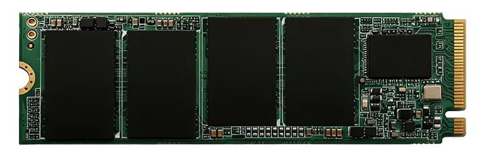
M.2 2280 NVMe SSD (With Cache) · Wide-temp
- Independent DRAM cache
- PCIe 3.0×4 lane
- Compatible with Industrial
M.2 2280 NVMe SSD (Cacheless) · Wide-temp
- PCIe 3.0×4 Lanes
- Supports TRIM/NCQ/S.M.A.R.T
- Compatible with Industrial
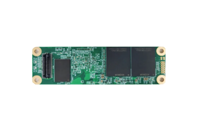
Rugged NVMe SSD
- Adopts Samtec high-speed
- PCIe Gen3×4 lanes
- Adopts Kioxia Industrial TLC
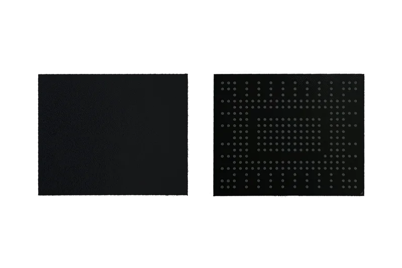
NVMe BGA SSD · Wide-temp
- FBGA291 Package
- PCIe Gen3×4 Interface
- Environmental testing
Related resources
Continue with related selection guides and notes for the same industrial memory topic.
Related cross-references
Pin-to-pin and functional alternatives referenced from this guide — for BOM review, dual-sourcing, or EOL coverage.